- Base Material: FR4/CEM3/CEM1/FR1/HighTG/LF/HF/High frequency/Al base/Cu base
- Max Board Size:1L 1800*800mm;2L 1200*600mm;≧4L 1200*600mm
- Copper thickness:1-12OZ
- Min line / space: 3/3mil
- Surface treatment:HASL,OSP,ENIG,Immersion Tin,Immersion Ag,Au plating
- Lead time: 1-3 days trial order,5-7 days for normal order
- Shipment:DHL/Fedex/UPS/TNT/EMS/AIR/SEA ect,Follow customers requirements
- SMD SMT DIP Component Assembly
A
small PCB refers to a compact
printed circuit board designed to fit within devices where space is limited. As electronics continue to shrink in size, the demand for small PCBs has grown significantly, especially in applications like
wearable devices, medical implants, IoT sensors, and compact consumer electronics.
Despite their reduced size, small PCBs require the same level of precision and functionality as larger circuit boards. Advanced
miniaturization techniques, high-density component placement, and multilayer stack-ups ensure that these PCBs maintain reliable performance in even the smallest devices.
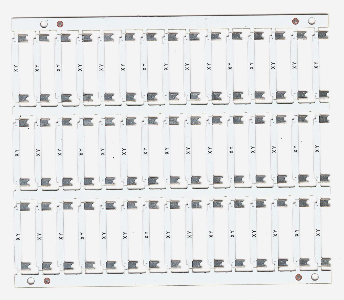
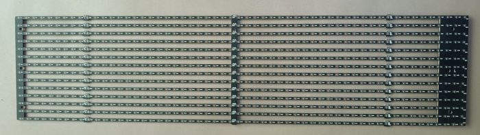
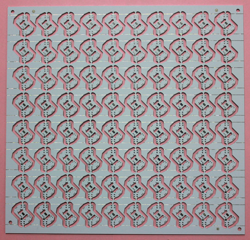
[caption id="attachment_2929" align="alignnone" width="300"]
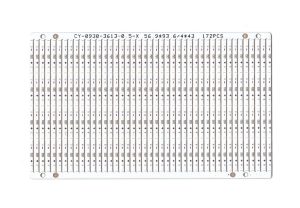
small PCB[/caption]
2. Characteristics
Small PCBS are designed for
efficiency, high-density circuitry, and lightweight construction. They often feature
fine-pitch components, micro vias, and flexible circuits to optimize space utilization. Due to their compact size, these PCBs require
precision manufacturing techniques, including laser drilling, advanced soldering processes, and surface-mount technology (SMT).
Another important aspect of small PCBs is their
thermal management. Since these boards are often used in devices with limited airflow, efficient heat dissipation strategies such as
thermal vias, metal-backed substrates, and copper pours are crucial to maintaining stability.
it can also be
rigid, flexible, or a combination of both (rigid-flex), depending on the application. Rigid-flex designs allow for
seamless integration into compact enclosures while maintaining signal integrity and mechanical durability.
3. Applications
Its are essential in various industries, particularly where
miniaturization and high performance are required. Some of the most common applications include:
- Wearable Technology: Smartwatches, fitness trackers, and health monitoring devices rely on small PCBs to integrate sensors, wireless connectivity, and power management into a compact form.
- Medical Devices: Pacemakers, hearing aids, and portable diagnostic tools use its for precision and reliability in life-saving applications.
- IoT and Smart Devices: Miniature PCBs power IoT sensors, smart home devices, and industrial automation equipment, enabling efficient data processing and communication.
- Consumer Electronics: Smartphones, Bluetooth earphones, and compact cameras require its to fit sophisticated circuitry into sleek and lightweight designs.
- Automotive Electronics: Advanced driver assistance systems (ADAS), electronic control units, and infotainment systems incorporate small PCBs to optimize performance in limited spaces.
4. Advantages
Its offer numerous benefits, making them ideal for modern electronic products. Their
compact size allows manufacturers to design
lighter, thinner, and more portable devices while maintaining high functionality.
Their
high-density component placement improves circuit efficiency, reducing signal loss and improving overall device performance. Additionally, Its are often
more energy-efficient, as they require lower power consumption compared to larger boards.
Another advantage is their
cost-effectiveness in mass production. With advanced PCB fabrication techniques, manufacturers can produce high-quality small PCBs with minimal material waste and high assembly precision.
Durability is also a key factor. Small PCBs are designed to withstand
vibration, mechanical stress, and harsh environments, making them suitable for applications in
automotive, aerospace, and industrial electronics.
5. Challenges in Design and Manufacturing
Despite their advantages, small PCBs present unique challenges in
design, fabrication, and assembly. One of the main difficulties is
component placement and routing, as limited space requires careful planning to avoid signal interference and thermal issues.
Manufacturing also demands
high-precision processes, such as laser drilling for micro vias, ultra-fine soldering techniques, and strict quality control to ensure
reliable connectivity and functionality.
Another challenge is
testing and debugging, as compact circuits make it difficult to probe and diagnose potential defects. Advanced inspection methods such as
X-ray imaging and automated optical inspection (AOI) are often required to detect hidden defects in small PCB assemblies.
To overcome these challenges, manufacturers must adopt
high-precision PCB fabrication technologies, use
advanced design software, and ensure strict
quality control measures throughout the production process.
6. Conclusion
Its are essential for
modern, compact electronic devices, providing
high performance, efficiency, and durability in a reduced footprint. With advancements in
miniaturization technology, flexible circuits, and high-density interconnects, small PCBs continue to push the boundaries of what is possible in electronics design.
For high-quality
small PCB manufacturing, Shuoqiang Electronics offers
custom PCB solutions tailored to meet the demands of
wearable tech, medical devices, IoT, and more. Contact us today for reliable fabrication and assembly services.
our
linkedin sqpcb.com 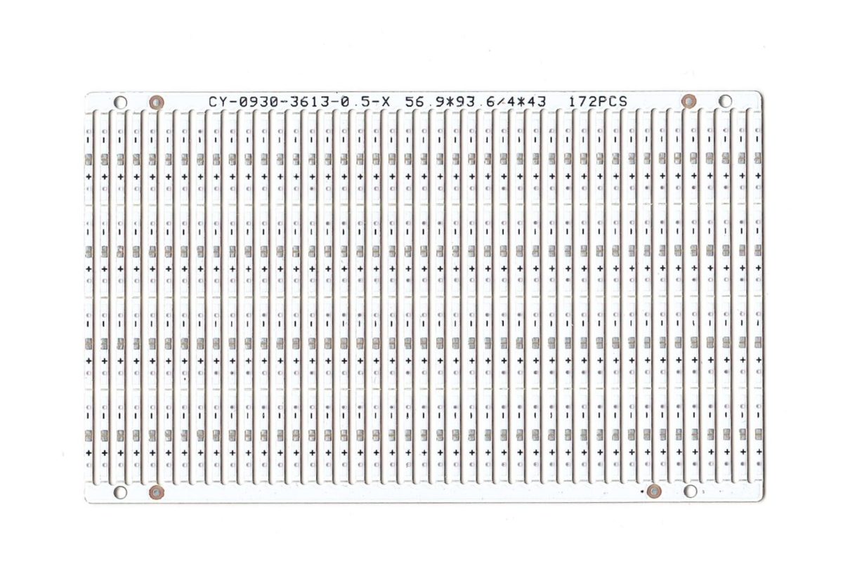

 Quote
Quote
 E-mail