- Base Material: FR4/CEM3/CEM1/FR1/HighTG/LF/HF/High frequency/Al base/Cu base
- Max Board Size:1L 1800*800mm;2L 1200*600mm;≧4L 1200*600mm
- Copper thickness:1-12OZ
- Min line / space: 3/3mil
- Surface treatment:HASL,OSP,ENIG,Immersion Tin,Immersion Ag,Au plating
- Lead time: 1-3 days trial order,5-7 days for normal order
- Shipment:DHL/Fedex/UPS/TNT/EMS/AIR/SEA ect,Follow customers requirements
- SMD SMT DIP Component Assembly
2 layers PCB (also known as a
double-sided PCB) is a
circuit board with
two conductive copper layers, one on the top and one on the bottom, separated by an insulating core material. Unlike single-layer PCBs, which have conductive traces only on one side,
2 layers PCB allow for more complex circuit designs, higher component density, and improved electrical performance.
This type of PCB is widely used in
consumer electronics, industrial control systems, medical devices, and automotive applications due to its
balance of cost, performance, and manufacturability.
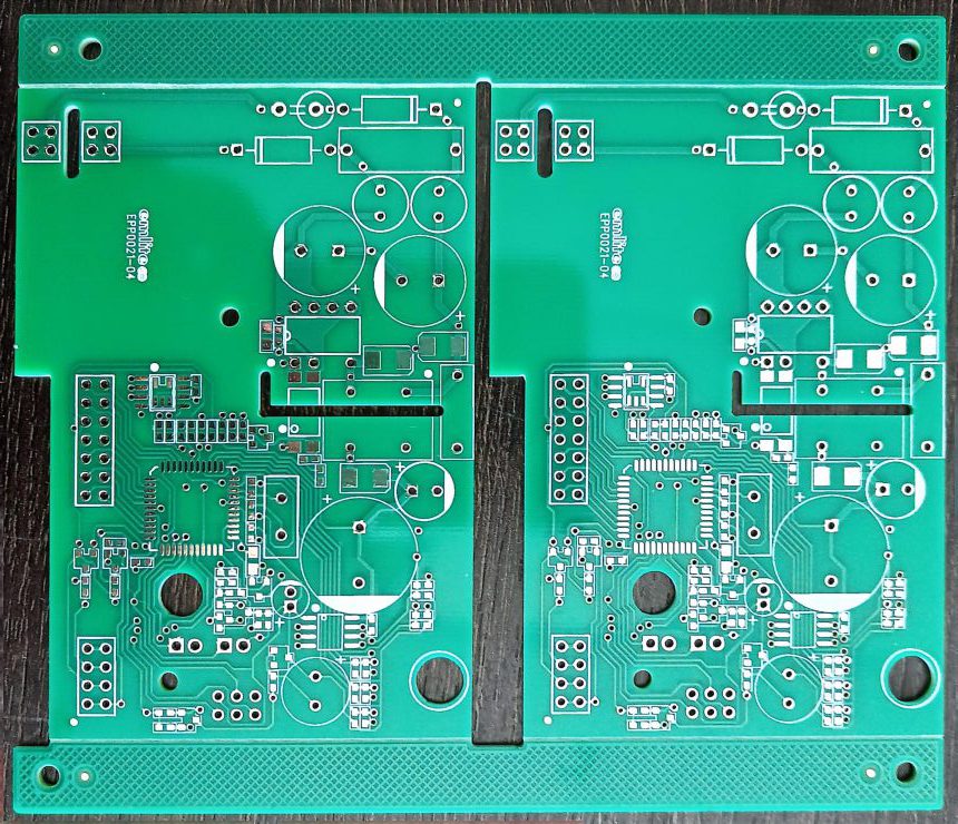
[caption id="attachment_2637" align="alignnone" width="300"]
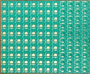
2 layers PCB[/caption]
2. Structure and Design of 2 layers PCB
A
2-layer PCB consists of multiple elements that enhance its functionality:
- Top and Bottom Copper Layers: These conductive layers enable electrical connections and signal transmission.
- Insulating Core (Substrate): Typically made of FR-4, this layer provides mechanical strength and electrical insulation.
- Vias (Through-Holes): These allow electrical connections between the top and bottom layers, enhancing circuit complexity.
- Solder Mask & Silkscreen: The solder mask protects the copper traces from oxidation and short circuits, while the silkscreen provides component markings.
Double-sided PCBs use
plated through-holes (PTH) or vias to connect the two layers, enabling more compact and functional circuit layouts compared to single-layer designs.
3. Advantages of 2 layers PCB
1. Increased Circuit Complexity
With conductive traces on both sides, 2-layer PCBs allow for more intricate circuit designs compared to single-layer boards. This makes them suitable for
higher-performance applications that require multiple connections and signal pathways.
2. Cost-Effective Compared to Multi-Layer PCBs
2-layer PCBs offer a good balance between
functionality and cost. They are
cheaper to manufacture than multi-layer PCBs, making them a preferred choice for
mid-range electronic products.
3. Compact and Lightweight Design
Since components can be placed on both sides,
2 layers PCB save space and reduce the overall size of the final product. This is especially useful for
portable devices and compact electronics.
4. Improved Electrical Performance
Compared to single-layer PCBs,
double-sided boards provide better signal routing and reduced interference, ensuring stable operation in
digital and analog circuits.
5. Easier Manufacturing and Assembly
The manufacturing process for
2-layer PCBs is simpler than that of multi-layer PCBs, leading to
faster production cycles and lower assembly costs.
4. Applications of 2 layers PCB
Due to their
versatility and affordability, 2-layer PCBs are used in a wide range of electronic devices and industries:
- Consumer Electronics: Smart home devices, audio equipment, wearables, and LED drivers.
- Industrial Equipment: Control panels, automation systems, and motor controllers.
- Medical Devices: Portable diagnostic tools, patient monitoring systems, and wearable health trackers.
- Automotive Electronics: Engine control modules, lighting systems, and infotainment units.
- Telecommunications: Wireless routers, modems, and network equipment.
The ability to mount components on both sides while maintaining
cost efficiency makes 2-layer PCBs an
ideal choice for medium-complexity electronics.
5. Challenges and Limitations of 2 layers PCB
While 2-layer PCBs offer
numerous benefits, they also come with some limitations:
- Limited Routing Space: Compared to multi-layer PCBs, 2-layer boards have fewer routing options, making them less suitable for very complex circuits.
- Signal Integrity Issues: High-speed or high-frequency applications may experience electromagnetic interference (EMI) and crosstalk, requiring careful design considerations.
- Less Thermal Management Capability: Without additional layers for heat dissipation, 2-layer PCBs may struggle with high-power components compared to metal-core or multi-layer designs.
Despite these challenges,
proper design techniques, such as ground planes and optimized trace layouts, can improve 2-layer PCB performance and reliability.
6. Conclusion
A
2 layers PCB is a
versatile, cost-effective, and widely used circuit board that provides
higher design flexibility and improved electrical performance compared to single-layer boards. It is a
preferred choice for mid-range applications, including
consumer electronics, industrial systems, medical devices, and automotive electronics.
While
multi-layer PCBs are necessary for high-performance applications,
2 layers PCB remain an excellent solution for many electronic products due to their
balance of functionality, manufacturability, and affordability.
For
custom 2 layers PCB manufacturing, Shuoqiang Electronics offers
high-quality PCB solutions with fast turnaround times and competitive pricing. Contact us today for
professional PCB design and fabrication services!
our
linkedin sqpcb.com


 Quote
Quote
 E-mail