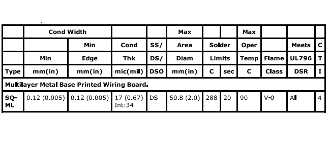
- Base Material: FR4/CEM3/CEM1/FR1/HighTG/LF/HF/High frequency/Al base/Cu base
- Max Board Size:1L 1800*800mm;2L 1200*600mm;≧4L 1200*600mm
- Copper thickness:1-12OZ
- Min line / space: 3/3mil
- Surface treatment:HASL,OSP,ENIG,Immersion Tin,Immersion Ag,Au plating
- Lead time: 1-3 days trial order,5-7 days for normal order
- Shipment:DHL/Fedex/UPS/TNT/EMS/AIR/SEA ect,Follow customers requirements
- SMD SMT DIP Component Assembly
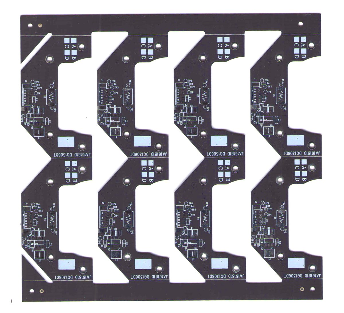
2 layers LED PCB, With the rapid advancement of LED technology, Printed Circuit Boards (PCBs) play a crucial role in ensuring optimal performance, heat dissipation, and efficiency. Among the various types of PCBs, 2-layer LED PCBs are widely used in lighting and electronic applications due to their reliability, cost-effectiveness, and thermal management capabilities. These PCBs allow for better electrical conductivity, enhanced thermal dissipation, and increased durability, making them an ideal choice for modern LED applications.
In this article, we will explore the structure, advantages, manufacturing process, and applications of
2-layer LED PCBs in detail.
[caption id="attachment_3085" align="alignnone" width="297"]
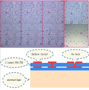
2 layers LED PCBs[/caption]
What is a 2 layers LED PCB?
A
2-layer LED PCB is a type of printed circuit board designed specifically for LED applications. It consists of two layers of conductive copper traces separated by an insulating dielectric material. Unlike single-layer PCBs, which have only one conductive layer,
2-layer PCBs offer better electrical performance, improved heat dissipation, and greater design flexibility.
These PCBs are commonly used in LED lighting due to their ability to handle higher power loads while maintaining a compact and efficient design. The additional layer allows for more complex circuit designs, facilitating better signal integrity and current flow management.
Key Components of a 2 layers LED PCB
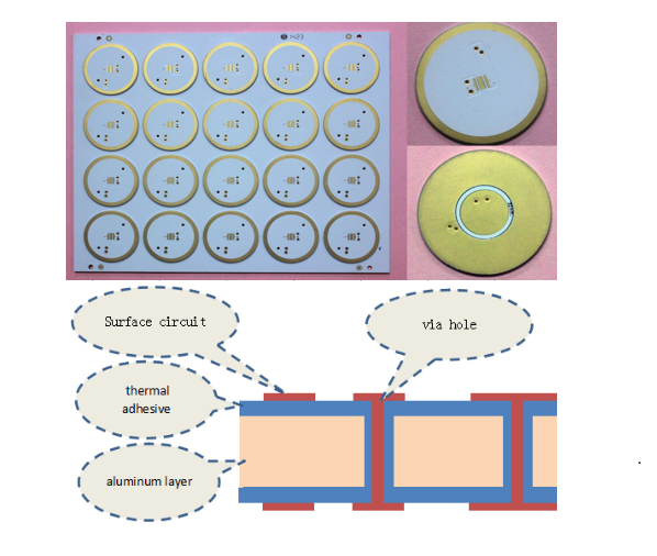
- Base Material – Typically made from FR4 (fiberglass-reinforced epoxy), aluminum, or metal-core PCB (MCPCB) materials for enhanced thermal conductivity.
- Copper Layers – Two conductive copper layers that allow for efficient power distribution and signal routing.
- Dielectric Layer – An insulating layer between the copper layers to prevent short circuits and improve electrical performance.
- Solder Mask – A protective coating that prevents oxidation and reduces the risk of solder bridging.
- Silkscreen Layer – Used to print markings, component identifiers, and other essential information to assist in assembly and troubleshooting.
Benefits of 2 layers LED PCB
1. Enhanced Thermal Management
One of the primary challenges of LED applications is heat dissipation. LEDs generate significant amounts of heat during operation, and poor thermal management can lead to reduced efficiency, color shifts, and even early failure.
2-layer LED PCBs, particularly those with aluminum or metal-core bases, offer superior heat dissipation, allowing heat to be transferred away from the LED components efficiently.
2. Higher Electrical Performance
The
dual-layer design allows for better signal integrity, lower electrical resistance, and increased power-handling capacity. By separating power and signal traces onto different layers, engineers can optimize the circuit layout, reduce interference, and improve overall performance.
3. Cost-Effectiveness
Compared to
multilayer PCBs,
2-layer LED PCBs are more affordable due to their simpler manufacturing process and lower material costs. They provide an excellent balance between
performance and budget, making them an attractive choice for a wide range of LED applications.
4. Improved Durability and Reliability
2-layer LED PCBs offer enhanced
structural integrity compared to single-layer boards. The additional copper layer reinforces the board, making it more resistant to mechanical stress and environmental factors such as moisture and temperature fluctuations. This ensures a
longer lifespan for LED products.
5. Compact and Lightweight Design
The
double-layer configuration enables designers to create compact, space-efficient circuit layouts, making them ideal for LED applications with size constraints, such as
automotive lighting, consumer electronics, and wearable LED gadgets.
Manufacturing Process of 2 layers LED PCB
The production of a
2-layer LED PCB involves several critical steps, ensuring
precision, reliability, and durability.
1. PCB Design and Layout
Engineers use
specialized PCB design software such as
Altium Designer, Eagle, or KiCad to create an optimized circuit layout. Proper design considerations are made to ensure
efficient signal flow, heat dissipation, and power distribution.
2. Material Selection
The choice of base material significantly impacts the performance of the PCB.
FR4 is commonly used for general applications, while
aluminum and metal-core PCBs (MCPCBs) are preferred for high-power LED applications requiring better thermal management.
3. Printing and Etching
The copper layers are laminated onto the base material, and the circuit pattern is printed using
photolithography.
Unwanted copper is then etched away, leaving behind the necessary conductive traces.
4. Drilling and Plating
Holes are drilled for
component mounting and vias, which are then plated with conductive materials to establish electrical connectivity between the layers.
5. Solder Mask Application
A protective
solder mask layer is applied to prevent oxidation and to minimize the risk of short circuits or solder bridging during assembly.
6. Silkscreen Printing
Component labels, part numbers, and other essential markings are printed onto the PCB using
silkscreen printing for easy identification and assembly guidance.
7. Surface Finishing
To improve solderability and protect the copper traces, the PCB undergoes
surface finishing treatments such as:
- HASL (Hot Air Solder Leveling)
- ENIG (Electroless Nickel Immersion Gold)
- OSP (Organic Solderability Preservative)
8. Component Assembly
LEDs and other electronic components are mounted onto the PCB using
Surface Mount Technology (SMT) or
Through-Hole Technology (THT), depending on the application requirements.
9. Quality Inspection and Testing
Before shipping,
strict quality control measures such as
automated optical inspection (AOI), X-ray testing, and functional tests are performed to ensure the PCB meets all
performance and safety standards.
Applications of 2-Layer LED PCBs
Due to their efficiency, thermal management, and reliability,
2-layer LED PCBs are widely used across various industries:
1. LED Lighting Systems
- Street lights for urban infrastructure
- Indoor and outdoor LED panels for home and commercial use
- Smart lighting solutions for energy efficiency
2. Automotive LED Applications
- Headlights and taillights for better visibility
- Dashboard displays and indicators
- Signal and brake lights
3. Consumer Electronics
- LED televisions and displays
- Smart home devices like LED-enabled thermostats and security systems
- Wearable LED gadgets for fashion and health monitoring
4. Medical Devices
- Surgical lighting systems
- Medical imaging equipment
- UV sterilization devices for disinfection
5. Industrial and Commercial Lighting
- Factory lighting for improved workspace visibility
- Display signage and advertising boards
- Retail lighting solutions
Conclusion
2 layers LED PCB or 2-layer LED PCBs offer a perfect balance of
cost, performance, and thermal efficiency, making them a preferred choice in the LED industry. Their
superior heat dissipation, electrical performance, and durability ensure
reliable LED applications across various sectors.
For high-quality
2-layer LED PCBs, partnering with an experienced manufacturer like
Shuoqiang Electronics ensures
exceptional performance, customized solutions, and superior reliability. Contact us today to discuss your
LED PCB requirements!
our
linkedin sqpcb.com

 Quote
Quote
 E-mail