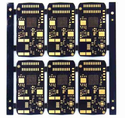
Printed Circuit Boards (PCBs) are the backbone of modern electronic devices, enabling complex circuits to be compactly and reliably implemented. The manufacturing of PCBs involves numerous intricate steps to ensure precision and functionality. Here, we break down the 17 common manufacturing processing steps involved in PCB production:
1. PCB Production, Design and Layout
The process begins with the design and layout of the PCB using specialized software (like Eagle, Altium, or KiCad). This includes creating schematics and defining the board’s physical dimensions, layer stack-up, and placement of components.
2. PCB Production, Printing the Design
Once the design is finalized, the next step is to print the PCB layout onto a transparent film. This film will serve as a template for subsequent steps in the manufacturing process.
3. PCB Production, Creating the Substrate
The substrate forms the foundation of the PCB. Typically, it is made of fiberglass (FR4) that is pre-coated with a layer of copper on both sides. This provides the base on which the circuit is built.
4. PCB Production, Transferring the Design
The PCB design is transferred onto the substrate through a process called photolithography. A photosensitive coating is applied to the copper substrate, and then it is exposed to UV light through the printed film. The exposed areas harden while the unexposed areas remain soft and are later washed away.

pcb production
5. PCB Production, Etching
Etching involves removing the unwanted copper from the board. The board is submerged in an acidic solution that dissolves the unprotected copper, leaving behind the desired copper traces.
6. PCB Production, Drilling
Precision drilling is performed to create holes for through-hole components and vias. Advanced machines are used to ensure accuracy, as these holes must align perfectly with the design specifications.
7. PCB Production, Plating
After drilling, the holes are plated with copper to ensure electrical connectivity between different layers of the PCB. This involves immersing the board in a copper plating solution and using an electrical current to deposit copper inside the holes.
8. PCB Productio, Applying the Solder Mask
A solder mask is applied to protect the copper traces from oxidation and to prevent solder bridges during component soldering. The solder mask is typically a green epoxy that is applied over the entire board, except for the pads where components will be soldered.
9. Silkscreen Application
The silkscreen layer is applied to add labels, symbols, and component identifiers to the PCB. This step involves applying a white ink to the board, which helps in assembling and identifying components during and after production.
10. Surface Finish
A surface finish is applied to the exposed copper areas to prevent oxidation and ensure solderability. Common finishes include HASL (Hot Air Solder Leveling), ENIG (Electroless Nickel Immersion Gold), and OSP (Organic Solderability Preservatives).
11. Electrical Testing
Electrical testing is conducted to ensure there are no shorts or open circuits on the PCB. Flying probe testers or bed-of-nails fixtures are used to verify the electrical integrity of the circuit.
12. Cutting and Routing
The PCBs are cut from the larger manufacturing panel into individual units. Routing is also performed to create specific shapes and to cut out any internal slots or complex contours.
13. Inspection
Visual inspection and automated optical inspection (AOI) are carried out to check for defects such as solder bridges, missing components, or incorrect placement. X-ray inspection may also be used for multilayer PCBs.
14. Component Mounting
Components are mounted onto the PCB using either through-hole or surface-mount technology (SMT). SMT involves placing components on the surface of the board and soldering them, whereas through-hole mounting involves inserting component leads through holes in the board and soldering them on the opposite side.
15. Soldering
Reflow soldering is used for SMT components. The PCB is passed through a reflow oven where the solder paste melts and forms joints. For through-hole components, wave soldering is commonly used.
16. Cleaning
Post-soldering, the PCBs are cleaned to remove any flux residues and contaminants that could affect performance or reliability. Cleaning methods include aqueous, semi-aqueous, and solvent-based processes.
17. Final Testing and Quality Control
Final testing involves functional testing to ensure that the PCB operates as intended. This may include in-circuit testing (ICT), functional testing, and burn-in testing to simulate real-world operating conditions. Any identified defects are rectified, and the boards undergo a final quality check before packaging.
Conclusion
The manufacturing of PCBs is a meticulous process that requires precision at every step to ensure the functionality and reliability of the final product. Understanding these 17 common processing steps provides insight into the complexity and technical expertise involved in producing high-quality PCBs that power the modern world of electronics.
- long board pcb
- Flexible PCBs
- Special PCB
- Express Printed Circuit Board
- Pcb Prototype
- LED PCB
- PCB
- Printed Circuit Board
- Pcb meaning
- Pcb manufacturer
- Rigid pcb board
- Rigid Flex PCB

 Quote
Quote
 E-mail