PCB manufacturing is not only about producing the final board. Before a PCB reaches component assembly, manufacturers need reliable ways to verify whether the fabrication process has achieved the required electrical, mechanical, and material performance. This is where PCB Test Coupons become valuable.
A well-designed test coupon provides a practical method for monitoring critical manufacturing parameters without testing every feature of the finished PCB destructively. For high-density, multilayer, high-speed, and high-reliability boards, this additional verification step can help identify process problems before they become expensive assembly or field failures.
What Are PCB Test Coupons?
PCB Test Coupons are small representative sections fabricated alongside the production PCB panel. They reproduce selected characteristics of the actual board, such as copper structures, plated through-holes, microvias, controlled-impedance traces, dielectric constructions, or multilayer interconnections. After fabrication, these sections can be tested to evaluate whether the manufacturing process meets specified requirements.
Depending on the application, a coupon may be used for microsection analysis, plating thickness verification, via reliability testing, impedance testing, solderability evaluation, or thermal-stress assessment. The exact coupon structure should be designed around the risks and specifications of the actual PCB rather than treated as a generic add-on.
In my view, the greatest value of a coupon is that it converts manufacturing quality from something that is simply assumed into something that can be measured. A production board may look perfect visually while hidden problems exist inside plated holes, copper layers, or dielectric structures. A properly designed coupon gives manufacturers another way to discover those risks before final assembly.
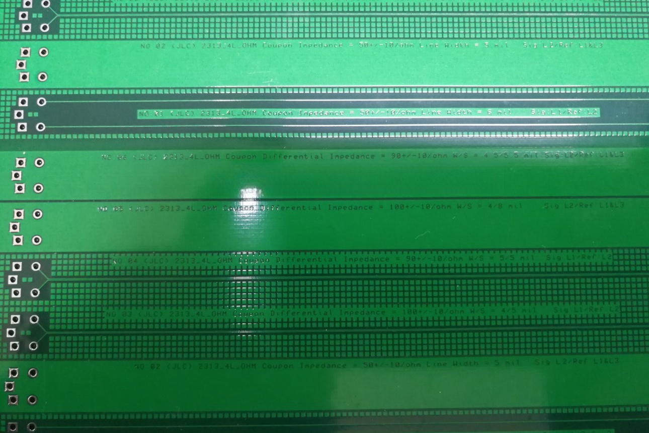
PCB Test Coupons
Why PCB Test Coupons Matter in Manufacturing
Modern PCBs often contain very small geometries and increasingly complex layer structures. A slight variation in copper thickness, drilling, plating, etching, lamination, or dielectric thickness can affect electrical performance and long-term reliability.
For example, insufficient copper plating in a via can reduce current-carrying capability and create a potential reliability concern during thermal cycling. Variations in dielectric thickness or trace geometry can also influence controlled impedance and high-speed signal performance. These problems may not be obvious from a conventional visual inspection.
Using a coupon allows manufacturers to examine representative structures under controlled testing conditions. If a coupon reveals excessive plating variation, poor interlayer bonding, dimensional deviations, or impedance problems, the process can be investigated and corrected before the finished boards move into assembly.
This is particularly important when the cost of a PCB failure extends beyond the bare board. A fabrication problem discovered after component placement may involve additional labor, component loss, rework, testing, and schedule delays.
PCB Test Coupons: Cost Factors and Performance Impact
The cost of implementing a coupon program is generally influenced by its design complexity, additional panel area, testing method, material requirements, and destructive analysis requirements. A simple electrical coupon may require relatively little additional manufacturing effort, while advanced impedance structures or microsection analysis can involve more testing and engineering resources.
There is also an indirect cost consideration. Allocating panel space to coupons may slightly affect material utilization, especially for smaller production panels. However, this should be considered against the potential cost of discovering a process problem only after assembly.
| Factor | Potential Impact |
|---|---|
| Coupon design | Engineering and setup cost |
| Additional panel area | Slightly higher material consumption |
| Microsection analysis | Additional laboratory and inspection cost |
| Impedance testing | Test equipment and measurement cost |
| Plating verification | Helps control via and hole reliability |
| Process monitoring | Can reduce scrap and rework |
From a performance perspective, coupons do not directly improve the PCB itself. Their value comes from verifying and controlling the processes that determine PCB performance. Better process verification can contribute to stable impedance, reliable vias, consistent plating, stronger interlayer connections, and improved manufacturing consistency.
PCB Test Coupons: Common Problems and Solutions
One common problem is designing a coupon that does not actually represent the most critical features of the production board. If the coupon structure is significantly easier to manufacture than the real PCB, passing the coupon test may provide limited assurance.
The solution is to develop coupon structures based on the actual manufacturing risks. For example, if the PCB contains fine-pitch vias or demanding high-speed impedance requirements, the coupon should include representative structures where appropriate.
Another issue is incorrect coupon placement or insufficient testing criteria. A coupon positioned in a way that does not adequately reflect panel-level process variation may produce misleading results. Manufacturers should therefore establish clear locations, test methods, acceptance criteria, and inspection procedures before production begins.
Testing itself can also create challenges. Destructive tests such as microsectioning provide valuable information but consume the tested coupon. For this reason, manufacturers need to determine which tests are necessary based on PCB specifications, customer requirements, and reliability expectations.
PCB Test Coupons: When Should They Be Used?
Not every PCB requires the same level of coupon testing. The need generally increases with board complexity, performance requirements, reliability expectations, and manufacturing risk.
Coupons are particularly useful for multilayer PCBs, HDI boards, high-speed designs, heavy-copper boards, impedance-controlled circuits, automotive or industrial electronics, and other applications where hidden manufacturing defects could have significant consequences.
For simpler boards with well-established manufacturing processes, the coupon requirements may be more limited. The important point is to match the testing strategy with the actual risk rather than adding unnecessary testing simply for the sake of testing.
PCB Test Coupons: A Practical Quality Strategy
The most effective approach is to treat coupons as part of a broader manufacturing quality system rather than as an isolated inspection step. Design engineering, PCB fabrication, quality control, and the customer should agree on what the coupon needs to verify before production begins.
At SQ PCB, this type of process-oriented thinking is important because PCB quality depends on many interconnected manufacturing stages. A coupon can help provide evidence that critical processes such as drilling, plating, lamination, etching, and impedance control are operating within the required range.
My perspective is simple: the earlier a manufacturing risk is identified, the less expensive it usually is to correct. A relatively small investment in representative testing can provide useful process information before a problem reaches component assembly or the customer’s final product.
Conclusion
PCB quality is determined by much more than whether the finished board passes a visual inspection. Internal copper structures, plated holes, dielectric characteristics, layer alignment, and electrical properties can all influence the reliability and performance of the final product. These characteristics are not always visible from the outside, which makes process verification particularly important.
PCB Test Coupons provide manufacturers with a practical way to examine representative structures and identify potential fabrication problems before they become assembly failures or field reliability issues. Their cost should therefore be viewed not simply as an additional manufacturing expense, but as part of a broader strategy for controlling quality, reducing rework, and improving production consistency.
For PCB buyers, engineers, and manufacturers, the key question is not simply whether a coupon is included. It is whether the coupon represents the critical characteristics of the actual PCB and whether the resulting test data can support meaningful process decisions. When designed and applied correctly, coupons can become an important bridge between PCB specifications and measurable manufacturing quality.
FAQs
1. What is the main purpose of a PCB test coupon?
A test coupon is used to evaluate selected PCB manufacturing characteristics, such as plating, vias, impedance, layer bonding, and dimensional consistency, without testing the entire production board destructively.
2. Are PCB test coupons required for every PCB?
No. Requirements depend on the PCB’s complexity, application, customer specifications, reliability requirements, and manufacturing risks. More complex and high-reliability boards generally benefit more from detailed coupon testing.
3. What can be tested using a PCB test coupon?
Depending on its design, a coupon can support tests for copper and plating thickness, via structures, impedance, dielectric construction, interlayer bonding, thermal reliability, and other fabrication characteristics.
4. Do test coupons increase PCB manufacturing costs?
They can add some engineering, material, and testing costs. However, they may help reduce larger expenses associated with scrap, rework, assembly failures, and late-stage quality problems.
5. How should a PCB test coupon be designed?
The coupon should represent the critical manufacturing characteristics of the actual PCB. Its structure and testing requirements should be determined according to the board’s layer construction, via technology, impedance requirements, materials, and reliability expectations.

- Special PCB
- long board pcb
- Flexible PCBs
- Special PCB
- Express Printed Circuit Board
- Pcb Prototype
- LED PCB
- PCB
- Pcb Meaning
- Printed Circuit Board
- Pcb manufacturer
- Rigid pcb board
 Quote
 E-mail