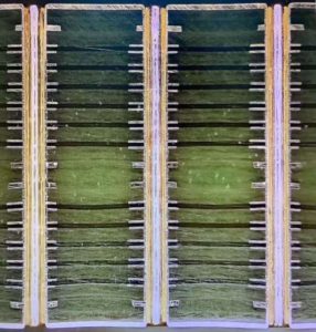
PCB Structure: A Comprehensive Guide to Printed Circuit Board Layers and Composition
Introduction
Printed Circuit Boards (PCBs) serve as the foundation for nearly all electronic devices, providing electrical connectivity and mechanical support for components. Understanding PCB structure is essential for engineers, manufacturers, and designers aiming to optimize performance, reliability, and efficiency.
This article explores the fundamental PCB structure, detailing its layers, materials, functions, and design considerations.

Complex Circuit Board pcb structure
Basic PCB Structure
A PCB consists of multiple layers, each serving a specific function. The primary components include:
- Substrate (Base Material)
- Copper Layer
- Solder Mask
- Silkscreen (Legend Layer)
- Vias and Holes
These elements work together to create a functional circuit, allowing for signal transmission and mechanical stability.
Layers of a PCB
1. Substrate (Base Material)
The base material provides the structural integrity of the PCB and determines its electrical and thermal properties.
- FR-4 (Fiberglass Epoxy Resin): The most common material, offering good electrical insulation and mechanical strength.
- Polyimide: Used for flexible PCBs, offering high thermal resistance.
- Metal Core (Aluminum or Copper): Ideal for high-power applications requiring superior heat dissipation.
- Ceramic: Used in specialized applications like aerospace and high-frequency electronics.
2. Copper Layer
The copper layer forms the conductive pathways on the PCB. Depending on the board type, the number of copper layers varies:
- Single-layer PCB: One copper layer (used in simple circuits)
- Double-layer PCB: Copper layers on both sides (used in more complex applications)
- Multi-layer PCB: Three or more copper layers (used in high-performance and compact devices)
Copper thickness is measured in ounces per square foot (oz/ft²), with common thicknesses being 1oz, 2oz, and 3oz, depending on the current-carrying requirements.
3. Solder Mask Layer
The solder mask is a protective layer applied over the copper traces to prevent oxidation, solder bridges, and short circuits.
- Green solder mask is the most common, but other colors like blue, black, and red are available.
- The solder mask opening exposes areas where components are soldered.
4. Silkscreen Layer (Legend Layer)
The silkscreen layer contains printed text and symbols to help identify components, part numbers, and test points. It is typically white and applied using inkjet or screen printing methods.
5. Vias and Holes
Vias are small holes drilled into the PCB to electrically connect different layers.
- Through-Hole Via: Passes through the entire PCB, connecting all layers.
- Blind Via: Connects an external layer to an internal layer without passing through the entire board.
- Buried Via: Connects internal layers only, without appearing on the outer surface.
- Microvia: Used in HDI (High-Density Interconnect) PCBs, enabling compact designs.
Types of PCB Structures
1. Single-Layer PCB
- One copper layer with components on one side.
- Simple and cost-effective.
- Used in basic circuits like power supplies and LED boards.
2. Double-Layer PCB
- Copper layers on both sides.
- Increased circuit complexity with vias connecting both layers.
- Commonly used in consumer electronics and automotive applications.
3. Multi-Layer PCB
- Three or more copper layers stacked together.
- More complex routing with internal signal, power, and ground layers.
- Found in computers, medical devices, and telecommunications equipment.
4. Rigid PCB
- Made from a solid FR-4 substrate.
- Maintains shape and durability.
- Used in industrial, aerospace, and automotive applications.
5. Flexible PCB (FPC)
- Uses polyimide or polyester substrates.
- Bendable and lightweight.
- Found in wearable devices, medical implants, and foldable phones.
6. Rigid-Flex PCB
- Combines rigid and flexible sections.
- Provides mechanical stability with flexible interconnections.
- Used in compact, high-performance electronics like military and aerospace applications.
7. Metal-Core PCB (MCPCB)
- Uses aluminum or copper as a heat-spreading layer.
- Improves thermal management for LED lighting, automotive, and power electronics.
Key Design Considerations for PCB Structure
1. Layer Stack-Up Design
Proper layer stack-up affects signal integrity, thermal performance, and EMI/EMC compliance.
- 4-layer PCB: Common in complex circuits, providing power and ground planes.
- 6-layer PCB: Adds extra routing layers for high-speed signals.
- HDI PCBs: Use microvias and stacked layers for compact designs.
2. Trace Width and Spacing
- Determines current-carrying capacity and impedance control.
- IPC-2221 standard provides guidelines for trace width calculations.
3. Thermal Management
- Heat dissipation techniques include thermal vias, metal cores, and copper pours.
- Essential for power electronics and high-speed circuits.
4. Signal Integrity and EMI Control
- Ground planes, differential pair routing, and shielding techniques reduce noise.
- High-frequency applications use controlled impedance routing.
5. Manufacturing Constraints
- Minimum drill sizes, trace widths, and via diameters depend on fabrication capabilities.
- DFM (Design for Manufacturability) ensures smooth production without defects.
Future Trends in PCB Structure
1. High-Density Interconnect (HDI) PCBs
- Uses laser-drilled microvias and finer trace widths.
- Found in smartphones and IoT devices.
2. Flexible Hybrid Electronics (FHE)
- Integrates flexible PCBs with printed electronic components.
- Enables ultra-lightweight and stretchable circuits.
3. Embedded Components
- Active and passive components integrated within PCB layers.
- Reduces size and improves signal performance.
4. Advanced Materials
- Low-loss laminates for 5G and high-speed computing.
- Environmentally friendly PCB materials reducing hazardous substances.
Conclusion
The PCB structure plays a fundamental role in electronic circuit design and performance. By understanding different layers, materials, and design considerations, engineers can optimize PCB reliability, efficiency, and manufacturability.
With emerging trends such as HDI, embedded components, and flexible hybrid electronics, the PCB industry is evolving to meet the demands of next-generation technologies. As electronic devices become smaller and more powerful, advancements in PCB structure and materials will continue to drive innovation in various industries, including consumer electronics, automotive, medical, and aerospace.
- long board pcb
- Flexible PCBs
- Special PCB
- Express Printed Circuit Board
- Pcb Prototype
- LED PCB
- PCB
- Printed Circuit Board
- Pcb meaning
- Pcb manufacturer
- Rigid pcb board
- Rigid Flex PCB

 Quote
Quote
 E-mail