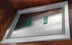
PCB stencil stencil for PCBA, In PCB manufacturing, a stencil is a crucial production tool designed to apply solder paste onto printed circuit boards (PCBs) with high precision. It is typically made of a high-strength metal mesh, such as stainless steel or nickel, and is meticulously designed to ensure accurate and consistent solder paste deposition. Stencils play a fundamental role in surface mount technology (SMT) assembly, enhancing production efficiency and reliability.
PCB stencil
The Function of Stencil in PCB Manufacturing
- Solder Paste Deposition Control
The primary function of a PCB stencil is to regulate the amount of solder paste applied to the PCB. The openings in the stencil allow solder paste to pass through and deposit onto the pads where electronic components will be soldered. The precise control of aperture size, shape, and distribution ensures optimal connectivity and minimizes defects like solder bridges and insufficient solder joints. - Accurate Component Placement
During the assembly process, components must be positioned precisely on designated solder pads. The stencil ensures that solder paste is applied only where necessary, aligning with the PCB layout. This accuracy enhances automated pick-and-place efficiency and prevents misalignment during reflow soldering. - Enhanced Production Efficiency and Consistency
PCB stencils enable rapid and uniform solder paste application, significantly improving manufacturing speed. Their high repeatability ensures consistency across multiple boards, which is essential for mass production. By using stencils, manufacturers can maintain a stable production line and control product quality efficiently.
The PCB Stencil Production Process
- Design and Layout Preparation
The stencil design is based on the PCB layout, considering pad sizes, component placements, and paste volume requirements. CAD software is used to create a precise template. - Material Selection and Frame Preparation
Stencils are usually made from stainless steel or nickel due to their durability and resistance to corrosion. Depending on the application, stencils may be framed or frameless. - Laser Cutting or Electroforming
The most common method for creating stencil openings is laser cutting, which offers high precision and smooth aperture walls. Electroforming, a chemical-based process, is another option for extremely fine-pitch components. - Post-Processing and Cleaning
After cutting, the stencil undergoes post-processing to remove burrs and enhance aperture quality. It is then cleaned to eliminate residual contaminants, ensuring optimal paste transfer. - Coating and Testing
Some stencils receive nano-coatings to reduce solder paste adhesion and improve release efficiency. Before use, the stencil is tested for alignment and accuracy to meet quality standards.
Advantages and Disadvantages of PCB Stencils
Advantages:
- High Precision: Stencils offer precise solder paste deposition, reducing defects and enhancing soldering quality.
- Durability: Made from robust materials, stencils can be used multiple times without degradation.
- Efficiency: The automated application of solder paste improves production speed and reduces labor costs.
- Consistency: Ensures uniform paste application across multiple PCBs, crucial for mass production.
Disadvantages:
- Initial Cost: High-quality stencils require investment in design and manufacturing.
- Limited Flexibility: Any design modifications necessitate creating a new stencil, which can be time-consuming and costly.
- Maintenance Required: Regular cleaning and handling are needed to prevent clogging and ensure long-term usability.
Types of PCB Stencils
- Framed Stencils
These stencils are mounted onto a frame for added support and rigidity. They are commonly used in high-volume production where durability and stability are crucial. - Frameless Stencils
Designed for cost-effectiveness and flexibility, frameless stencils require a reusable tensioning system. They are suitable for prototype and low-to-medium volume production. - Electroformed Stencils
Manufactured through electroforming, these stencils have superior paste release properties, making them ideal for ultra-fine pitch applications. - Nano-Coated Stencils
Stencils treated with nano-coatings enhance paste release efficiency and reduce cleaning frequency, improving overall production efficiency.
Conclusion
PCB stencils are indispensable in modern electronics manufacturing, facilitating precise solder paste deposition, ensuring accurate component placement, and enhancing production efficiency. By understanding their functions, advantages, and types, manufacturers can optimize their PCB assembly processes, achieving higher quality and reliability in electronic devices.

- long board pcb
- Flexible PCBs
- Special PCB
- Express Printed Circuit Board
- Pcb Prototype
- LED PCB
- PCB
- Printed Circuit Board
- Pcb meaning
- Pcb manufacturer
- Rigid pcb board
- Rigid Flex PCB
 Quote
Quote
 E-mail