A PCB panel is a crucial part of the PCB manufacturing process, serving as the foundation for efficiently producing multiple circuit boards. Whether you’re working with rigid, flexible, or rigid-flex PCBs, the design and optimization of the PCB panel directly impact the production speed, cost, and overall quality. In this article, we will dive deep into PCB panels, covering everything from design guidelines to material choices, as well as the challenges faced during panelization.
PCB Panel
1. What Is a PCB Panel?
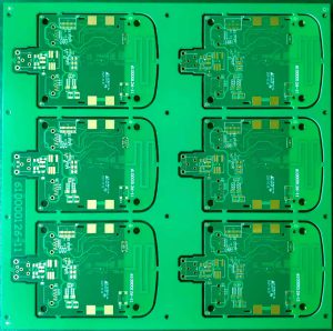
A PCB panel refers to a large sheet or board that holds multiple individual printed circuit boards (PCBs) for manufacturing. These panels help in improving the efficiency of the PCB production process by allowing multiple PCBs to be processed simultaneously. Essentially, they are designed to make the production line more effective, reducing handling time and cost per unit.
But here’s the kicker: PCB panels are not just about grouping boards together; they are carefully designed to maximize space and minimize waste. The process of panelizing involves placing PCBs on a larger board that can be handled easily during the manufacturing stages such as drilling, etching, and soldering. This panelized approach ensures that manufacturers can mass-produce PCBs more efficiently while maintaining high quality and reliability.
Table 1: Components of a PCB Panel
| Component | Description | Function |
|---|---|---|
| PCB Array | Multiple individual PCBs within a panel | Reduces handling time and cost |
| Routing Paths | Channels for separating individual PCBs post-manufacturing | Enables easy separation after production |
| V-Scoring | Pre-cut lines for easy breakage of individual PCBs | Simplifies post-manufacturing separation |
2. The Role of PCB-Panels in the PCB Manufacturing Process
PCB panels play a vital role in optimizing the overall manufacturing process. By combining multiple PCBs into a single panel, manufacturers can streamline the handling and processing stages. The panelization method allows for efficient use of raw materials, reducing scrap, and improving cost-effectiveness in mass production.
What’s the real story? Without proper panelization, each PCB would need to be processed separately, greatly increasing production time and costs. By using panels, manufacturers can test, etch, drill, and solder multiple boards at once, all while maintaining consistency and quality. The design of the PCB panel directly influences how quickly and efficiently these processes are carried out. The goal is always to maximize yield and minimize defects.
The design and choice of panel type, whether rigid or flexible, are influenced by factors such as the complexity of the PCB, the size of the product, and the final application of the circuit board.
Table 2: Impact of PCB Panel Design on Manufacturing Efficiency
| Design Feature | Effect on Manufacturing Efficiency | Key Benefit |
|---|---|---|
| Panel Size | Affects the number of PCBs per panel | Higher throughput, reduced cost |
| V-Scoring | Facilitates easy separation after production | Speed and precision in final assembly |
| Material Type | Influences durability and handling ease | Longer-lasting panels, fewer defects |
3. Types of PCB-Panels
PCB panels come in several types, each designed for specific needs within the manufacturing process. The primary types include rigid PCB panels, flexible PCB panels, and rigid-flex PCB panels. Each type offers unique benefits and is chosen based on the application, production volume, and required performance.
Ready for the good part? Let’s dive deeper into these different types of PCB-panels:
- Rigid PCB-Panels: These are the most commonly used panels, designed for standard rigid circuit boards. They provide robust support during the manufacturing process and are cost-effective for high-volume production.
- Flexible PCB-Panels: Used for flexible circuit boards, these panels allow for bending and conforming to a variety of shapes. Flexible PCB panels are commonly found in consumer electronics like wearables and mobile devices.
- Rigid-Flex PCB-Panels: Combining both rigid and flexible PCBs, these panels are used for complex applications where both rigidity and flexibility are required, such as in automotive and medical devices.
Table 3: Comparison of Different PCB Panel Types
| Panel Type | Application Area | Benefits |
|---|---|---|
| Rigid PCB Panels | Standard electronics, computers | Reliable, cost-effective, high-volume production |
| Flexible PCB Panels | Wearables, medical devices, mobile electronics | Flexible, lightweight, space-saving |
| Rigid-Flex PCB Panels | Aerospace, automotive, high-performance devices | Combines flexibility and rigidity for complex applications |
4. How to Choose the Right PCB-Panel for Your Project
Choosing the right PCB panel is critical for ensuring the efficiency and cost-effectiveness of your manufacturing process. There are several factors to consider, such as the type of PCB, material, and the specific requirements of your product.
What’s the real story? The right PCB panel not only impacts your production speed but can also influence your product’s final performance. Here are the key considerations when selecting the perfect PCB panel:
- Type of PCB: Decide whether you need a rigid, flexible, or rigid-flex PCB panel based on your end product’s requirements.
- Material Selection: Choose the material for the panel based on the mechanical and electrical properties needed. For instance, FR4 is a common material for rigid PCBs, while polyimide might be used for flexible panels.
- Production Volume: High-volume production benefits from large, standardized panels, while smaller runs might be better suited for flexible panels or even smaller rigid boards.
Table 4: Key Considerations for Selecting the Right PCB-Panel
| Factor | Consideration | Impact on Production |
|---|---|---|
| PCB Type | Rigid, flexible, or rigid-flex | Affects material choice and flexibility |
| Material | FR4, polyimide, etc. | Determines durability and performance |
| Volume | High or low production volume | Influences panel size and setup |
5. PCB-Panel Design Guidelines
Effective PCB panel design is essential to ensure manufacturability, functionality, and cost-efficiency. Design guidelines help minimize waste, ensure efficient use of materials, and optimize production timelines.
But here’s the kicker: the design of your PCB-panel can significantly influence both the initial cost and long-term success of your production process. Here are some key guidelines:
- Efficient Layout: Use the available panel space wisely by arranging multiple PCBs on the panel to maximize material usage and minimize waste.
- V-Scoring: Incorporating V-scoring or tab-routing into the panel design allows for easy separation of individual PCBs after manufacturing, streamlining the final stages of production.
- Minimizing Handling Issues: Ensure that the panel design is easy to handle, with appropriate edge connections and alignment guides to prevent damage during processing.
Table 5: Essential PCB Panel Design Guidelines
| Guideline | Description | Benefit |
|---|---|---|
| Efficient Layout | Maximize space on the panel | Reduce material waste, optimize throughput |
| V-Scoring | Include pre-scoring for easy separation | Simplifies assembly, prevents damage |
| Handling Considerations | Design for ease of handling and alignment | Reduces damage and increases production speed |
6. The Importance of Panel Layout Optimization
Panel layout optimization is one of the most critical aspects of PCB panel design. By effectively managing the arrangement of multiple PCBs, manufacturers can significantly reduce costs and improve production efficiency.
This is where it gets interesting: optimizing your panel layout doesn’t just save space; it ensures that every PCB is processed with minimal waste and maximizes the yield. Proper layout also minimizes the risk of defects, as it reduces the chances of manufacturing inconsistencies and testing failures.
Key strategies for layout optimization include:
- Maximizing Panel Utilization: Ensure the panel is fully utilized by arranging PCBs to minimize empty space.
- Testing Requirements: Take into account the testing methods used for the PCBs and design the panel to accommodate testing equipment, minimizing handling during inspection.
- Complexity of the PCB Design: The complexity of the PCB affects the layout. More complex designs may need to be spaced apart to ensure accurate manufacturing.
Table 6: Layout Optimization Strategies for PCB-Panels
| Strategy | Benefit | Application |
|---|---|---|
| Maximize Utilization | Reduces material waste, increases yield | Ideal for high-volume production |
| Testing Considerations | Accommodates testing equipment | Improves testing efficiency |
| Manage Complexity | Prevents defects and ensures accurate manufacturing | Suited for more complex PCB designs |
7. Materials Used for PCB-Panels
The material selected for the PCB panel has a direct impact on the performance, durability, and cost of the final product. The most commonly used materials for PCB panels include FR4, aluminum, and polyimide, each offering distinct advantages based on the application.
What’s the real story? The choice of material not only influences the mechanical properties of the PCB but also its thermal performance, electrical conductivity, and overall reliability. Choosing the right material for the panel is essential for achieving the desired performance and longevity of the PCB.
Table 7: Common Materials for PCB Panels
| Material | Application Areas | Benefits |
|---|---|---|
| FR4 | Standard electronics, consumer devices | Cost-effective, widely available |
| Aluminum | Power electronics, automotive applications | Excellent heat dissipation |
| Polyimide | Flexible PCBs, high-performance applications | High flexibility, thermal stability |
8. Advanced PCB-Panel Technologies
The PCB industry is constantly evolving, and with new technologies, PCB panel design is becoming more sophisticated. Innovations like automation, AI integration, and robotics are transforming how panels are designed, produced, and tested.
Ready for the good part? These technologies make it possible to produce more accurate, reliable, and cost-effective PCB panels, even in high-volume production settings. Automated systems reduce human error, AI optimizes panel layouts, and robotic systems speed up the manufacturing process, leading to increased efficiency and lower costs.
Table 8: Advanced Technologies in PCB Panel Production
| Technology | Description | Benefit |
|---|---|---|
| Automation | Use of automated systems in panel handling | Increases speed, reduces errors |
| AI Integration | AI-driven design and layout optimization | Enhances panel efficiency |
| Robotics | Robotic arms for handling and assembly | Reduces labor costs, improves precision |
9. Cost Considerations in PCB Panelization
Cost is always a critical factor in any manufacturing process, and PCB panelization is no exception. The cost of panelization depends on various factors, including the material, design complexity, and production volume.
What’s the real story? While initial setup costs for panelizing PCBs may seem higher, the long-term benefits of reduced per-unit cost, improved yield, and faster production can make it a worthwhile investment. When selecting the right panel design, it’s essential to weigh the initial costs against the potential savings in production.
Table 9: Cost Breakdown in PCB Panelization
| Cost Factor | Description | Impact on Total Cost |
|---|---|---|
| Material | Type of material used for the panel | Influences overall cost of production |
| Design Complexity | The complexity of panel layout | Affects tooling and setup time |
| Production Volume | Higher volumes typically reduce per-unit cost | Economies of scale reduce overall cost |
10. Conclusion
PCB panelization is a critical step in the PCB manufacturing process, impacting efficiency, cost, and quality. By selecting the right panel design, material, and layout, manufacturers can optimize their production processes, reduce waste, and improve their bottom line. Whether dealing with rigid, flexible, or rigid-flex PCBs, understanding the key considerations and best practices for PCB panels can ensure successful, cost-effective manufacturing.
FAQ
Q1: What is a PCB-panel?
A PCB panel is a large sheet that holds multiple individual PCBs, allowing for more efficient manufacturing and testing.
Q2: How does PCB panelization work?
PCB panelization involves arranging multiple PCBs on a single panel to streamline production, reduce costs, and improve testing efficiency.
Q3: What are the different types of PCB-panels?
The common types of PCB panels include rigid, flexible, and rigid-flex panels, each designed for specific applications and manufacturing requirements.
Q4: Why is PCB-panel layout optimization important?
Optimizing the layout helps maximize space, minimize waste, and ensure better yield during the manufacturing process.
Q5: How does panelization affect the cost of PCB manufacturing?
Panelizing PCBs reduces the cost per unit by allowing for efficient use of materials, faster production, and more consistent results across large batches.

- long board pcb
- Flexible PCBs
- Special PCB
- Express Printed Circuit Board
- Pcb Prototype
- LED PCB
- PCB
- Printed Circuit Board
- Pcb meaning
- Pcb manufacturer
- Rigid pcb board
- Rigid Flex PCB
 Quote
Quote
 E-mail