PCB overlays, also known as silkscreens, play a vital role in the design and manufacturing of printed circuit boards (PCBs). These overlays provide essential information directly on the PCB surface, helping with assembly, testing, maintenance, and troubleshooting. In this comprehensive guide, we will explore the functions of PCB overlays, their materials, design considerations, application processes, and best practices.
An essential component in PCB design, overlays are layers of printed ink on the PCB surface. These markings include component identifiers, test points, polarity indicators, logos, and other critical symbols that guide the assembly process and ensure proper functionality. Typically, PCB overlays are applied to the component side but can also be on the solder side when required. SQPCB ensures the highest-quality overlays with a focus on clarity, durability, and long-term reliability.
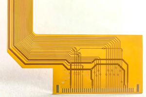
PCB Overlay
Functions of PCB Overlays
PCB overlays serve multiple critical functions:
-
Component Identification: Overlays label components with reference designators (e.g., R1, C2, U3), ensuring precise placement during assembly and aiding in troubleshooting.
-
Polarity and Orientation Indicators: Symbols such as polarity markers for diodes and electrolytic capacitors, or pin 1 indicators for ICs, help prevent incorrect installations.
-
Test Point Designation: Clearly marked test points help streamline the testing and debugging process.
-
Safety and Warning Labels: Overlays can include safety symbols to highlight areas with high voltage or other potential hazards.
-
Branding and Certification Marks: Logos, part numbers, revision levels, and certification marks (e.g., UL, CE) can be displayed for identification and compliance purposes.
Materials Used in PCB Overlays
For long-lasting PCB overlays, it is crucial to use the right materials. The commonly used materials include:
-
Inks: Epoxy and acrylic-based inks are typically used for their durability and resistance to high temperatures during soldering.
-
Substrates: While the overlay is printed on top of the solder mask layer, it’s important to ensure that the ink adheres properly to the solder mask for longevity.
Design Considerations for PCB Overlays
Effective PCB overlay design requires attention to several factors:
-
Clarity and Legibility: Use standardized fonts and sizes for easy readability. Small text may become illegible after printing, especially in high-density designs.
-
Placement: Position the overlay information to avoid covering critical areas such as solder pads or vias.
-
Layer Selection: Decide whether to place the overlay on the top layer, bottom layer, or both, based on component placement and board design.
-
Color Contrast: Choose contrasting ink colors that stand out clearly against the solder mask, improving visibility.
-
Manufacturing Constraints: Follow manufacturer specifications for minimum line widths, text heights, and spacing to ensure accurate printing.
Application Processes for PCB Overlays
Several methods can be used to apply overlays to PCBs manufacturing process:
-
Screen Printing: A traditional method where ink is pushed through a stencil onto the PCB surface. It’s ideal for large-scale production but may not provide the fine details required for complex designs.
-
Liquid Photo Imaging (LPI): A more accurate process where photosensitive ink is applied, exposed to UV light, and developed to create the desired pattern.
-
Direct Legend Printing (DLP): An advanced method using inkjet printing technology that applies the overlay directly onto the PCB. It’s highly flexible and provides high-resolution printing for intricate designs.
Best Practices for PCB Overlay Design
To ensure a functional and reliable PCB overlay, follow these best practices:
-
Standardization: Adhere to industry standards such as IPC-2221 for overlay design to ensure consistency and compatibility.
-
Avoid Overcrowding: Leave sufficient space between overlay elements to prevent confusion and ensure readability.
-
Alignment with Assembly Processes: Design overlays with automated assembly equipment in mind to avoid interfering with machine placement.
-
Environmental Considerations: Choose materials and designs that can withstand the operating environment, including temperature fluctuations, humidity, and exposure to chemicals.
Challenges in PCB Overlay Implementation
Several challenges come with implementing PCB overlays, including:
-
Registration Accuracy: Misalignment between the overlay and underlying PCB features can lead to errors in assembly. Precise registration during printing is crucial.
-
Durability: Overlays must resist abrasion, solvents, and thermal stress during soldering and operation.
-
Miniaturization: As PCBs become smaller, designing legible overlays that don’t interfere with electrical functionality becomes increasingly challenging.
Advanced Techniques in PCB Overlays
With advancements in technology, new techniques are being implemented to improve PCB overlays:
-
Multi-Color Overlays: Multiple ink colors are used to differentiate information and enhance the PCB’s aesthetic appeal.
-
Embedded QR Codes: Some PCBs now feature machine-readable QR codes for tracking and inventory management or for providing quick access to online resources.
-
Interactive Overlays: Some PCBs feature touch-sensitive overlays for specific applications, creating a more interactive user experience.
Case Study: PCB Overlay Design Optimization
In a case where PCB designs had multiple revisions due to assembly errors caused by unclear overlays, a redesign with larger, more legible fonts, clear polarity indicators, and distinct test point markings significantly reduced the error rate. This resulted in improved product reliability and reduced manufacturing costs.
Materials and Durability of PCB Overlays
To ensure durability, the materials selected for PCB overlays must withstand extreme conditions. Commonly used materials include epoxy-based inks, acrylic-based inks, and UV-curable inks, each offering specific benefits in terms of adhesion, chemical resistance, and durability.
Emerging Trends in PCB Overlays
The PCB industry is evolving with the integration of new technologies:
-
3D Printing: Some manufacturers are exploring 3D printing for raised overlays, enhancing durability and functionality.
-
Smart Overlays: Future PCBs might include smart overlays, such as RFID tags or augmented reality (AR) overlays, improving supply chain tracking and providing digital assembly guides.
Conclusion
PCB overlays play a crucial role in ensuring the functionality, reliability, and longevity of electronic devices. By adhering to best practices and leveraging advanced manufacturing techniques, manufacturers can design overlays that meet the evolving demands of modern electronics. With companies like SQPCB leading the way in high-quality overlay materials and innovative manufacturing processes, the future of PCB overlays looks bright, contributing to the continued advancement of electronic systems.
SQPCB not only provides superior quality overlays but also ensures that the most up-to-date techniques and materials are used to meet the stringent demands of today’s high-performance electronics.
Frequently Asked Questions (FAQ)
-
What is the function of PCB overlays?
PCB overlays provide essential markings for component identification, polarity indicators, test points, and safety labels, which aid in assembly, testing, and troubleshooting. -
What materials are commonly used for PCB overlays?
Common materials include epoxy-based inks, acrylic-based inks, and UV-curable inks, chosen for their durability, chemical resistance, and high-resolution printing capabilities. -
What are the challenges in designing PCB overlays?
Challenges include ensuring legibility, avoiding overcrowding, maintaining durability under harsh conditions, and meeting the precision required for miniaturized designs. -
How does SQPCB ensure high-quality PCB overlays?
SQPCB uses advanced manufacturing techniques such as liquid photo imaging (LPI) and precision inkjet printing to ensure overlays are clear, durable, and aligned correctly with PCB features. -
What are the emerging trends in PCB overlays?
Emerging trends include multi-color overlays, embedded QR codes, and interactive overlays, as well as the adoption of 3D printing and smart overlays that enable real-time tracking and enhanced functionality.

- long board pcb
- Flexible PCBs
- Special PCB
- Express Printed Circuit Board
- Pcb Prototype
- LED PCB
- PCB
- Printed Circuit Board
- Pcb meaning
- Pcb manufacturer
- Rigid pcb board
- Rigid Flex PCB
 Quote
Quote
 E-mail