In the microscopic world of printed circuit boards (PCBs), every hole serves a specific function. These holes are not only structural “anchors” but also the “blood vessels” for current transmission and signal connectivity. From basic vias to precise heat dissipation holes, the design of PCB holes directly impacts the performance and reliability of electronic devices. This article provides a comprehensive overview of the classification, functions, and manufacturing processes of PCB holes, integrating industry-leading practices from SQPCB to reveal the core logic of hole design.
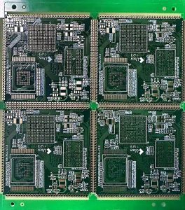
PCB Holes
1. Scientific Classification and Core Functions of PCB Holes
Strictly speaking, the holes in a PCB should be classified into three main types based on their functionality and structure: Vias, Insertion Holes, and Mounting Holes. Each type has specific technical definitions and application scenarios.
1.1 Vias: The “Invisible Bridges” of Circuits
Vias are metalized holes that traverse multi-layer PCBs, and their core function is to provide electrical connectivity between different layers of the circuit. Depending on their depth and connectivity, vias can be subdivided into:
- Through-Hole Via (THV): These vias penetrate the entire thickness of the PCB and are used to connect the top and bottom layers. They are the most common type of via.
- Blind Via: These vias only penetrate part of the PCB layers (e.g., from the top layer to a middle layer), commonly used in high-density interconnect (HDI) boards to reduce space usage.
- Buried Via: These vias are completely hidden within the multi-layer PCB (not exposed to the surface) and are typically used in high-end server motherboards or communication device boards to enhance signal integrity.
The hole walls of vias are copper-plated using chemical and electroplating processes to ensure stable current and signal transmission.
1.2 Insertion Holes: “Mechanical Anchors and Electrical Interfaces” for Components
Insertion holes are primarily used for soldering through-hole components (such as resistors, capacitors, and connectors). Their design needs to balance both mechanical strength and electrical performance:
- Metalized Processing: The hole walls are copper-plated (typically ≥25μm in thickness) to ensure reliable soldering of component leads to the PCB.
- Size Precision: The hole diameter must match the component lead diameter (tolerance ±0.05mm) to avoid issues like cold soldering or short circuits.
- Extended Functionality: Some insertion holes feature an “expanded mouth” design (such as a bell shape) to improve the yield rate during soldering.
1.3 Mounting Holes: “Physical Framework” for Device Assembly
Mounting holes are used to secure the PCB to the outer casing of the device. These are typically non-plated through holes (NPTH, Non-Plated Through Holes):
- No Copper Design: These holes do not have copper plating on the walls to prevent contact with the casing’s conductive parts, which could lead to a short circuit.
- Threaded Compatibility: The hole may be threaded (e.g., M3, M4) to accommodate screws or nuts, providing a robust mechanical fixing.
- Anti-Orientation Design: Some mounting holes are designed with non-circular shapes (e.g., oval) to prevent incorrect assembly or misalignment of the PCB.
2. Full Process Flow of PCB Hole Manufacturing: From Drilling to Surface Treatment
The functionality of PCB holes relies on precise manufacturing processes, with key steps including:
2.1 Drilling Formation
- CNC Drilling (Precision ±0.01mm): The initial hole is drilled using CNC drilling machines or laser drilling machines (used for micro-holes, diameter ≤0.1mm).
- Stacked Drilling for Multi-Layer Boards: In multi-layer boards, stacked drilling is employed to ensure precise hole alignment across layers (tolerance ≤0.05mm).
2.2 Metalization Process (Only for Vias/Insertion Holes)
- Chemical Copper Plating: A thin copper layer (approx. 0.5μm) is deposited on the hole walls to form the conductive base.
- Electroplating to Thicken Copper: Copper is electroplated onto the hole walls, with thickness ranging from 5-25μm, to meet current-carrying requirements.
2.3 Surface Treatment
- Solder Mask: A solder mask is applied to the non-solder areas to prevent short circuits. Common colors include green, red, and blue, with high-end products often using black or white for better visual differentiation.
- Functional Coatings: For insertion holes, “Hot Air Solder Leveling” (HASL) or “Electroless Nickel Immersion Gold” (ENIG) processes are used to ensure excellent solderability. Mounting holes may be coated with anti-corrosion oils (like OSP) to extend storage life.
3. SQPCB: Industry Leader in High-Precision Hole Processing
SQPCB (a leading PCB supplier) stands out in the PCB manufacturing field due to its deep understanding of hole processes, making it the partner of choice for high-end customers. The company’s core competencies include:
3.1 High-Density Hole Processing Capabilities
For high-precision requirements like 5G communication boards and IC substrates, SQPCB uses a “laser + mechanical” composite drilling technology. This allows for a full range of hole diameters (0.05mm-6.0mm), with hole position tolerance controlled within ±0.02mm (industry average ±0.05mm).
3.2 Metalization Quality Control
For complex structures such as blind and buried vias, SQPCB has introduced “plasma cleaning” pre-treatment technology to remove organic residues from the hole walls, ensuring uniform copper plating (thickness deviation <5%). Its vias have passed reliability tests such as thermal shock tests, achieving over 1000 cycles (industry standard is 500 cycles).
3.3 Customized Surface Treatment Solutions
Depending on application scenarios, SQPCB offers flexible surface treatment options:
- High-Frequency Boards (e.g., radar circuit boards): Uses “Silver Plating” (better conductivity than gold plating) to reduce signal loss.
- Automotive Electronics Boards: Employs “Electroless Nickel Immersion Gold (ENIG)” for enhanced soldering durability, with vibration resistance tests exceeding 500 hours.
4. Summary: Core Logic of Hole Design
The essential function of PCB holes is “connection”—whether it is electrical, mechanical, or structural. When choosing between vias, insertion holes, or mounting holes, factors such as:
- Electrical Performance: High-frequency signals should prioritize metalized vias (to reduce impedance).
- Mechanical Strength: Large components that require fixation need mounting holes (non-metalized).
- Space Constraints: High-density boards should use blind or buried vias to save space.
Looking forward, as technologies like AIoT and autonomous driving evolve, PCB holes will continue to evolve towards being “smaller, more precise, and more reliable.” PCB Suppliers with full-process hole manufacturing capabilities, will be key players in driving industry upgrades.
SEO Optimized Title: PCB Holes Explained: From Vias to Mounting Holes with SQPCB’s Expertise
Permalink: pcb-holes-vias-mounting-holes-sqpcb
Meta Description: Discover the different types of PCB holes, their functions, and the manufacturing processes involved. Learn how SQPCB ensures high precision in hole processing for advanced applications like 5G and automotive electronics.

- long board pcb
- Flexible PCBs
- Special PCB
- Express Printed Circuit Board
- Pcb Prototype
- LED PCB
- PCB
- Printed Circuit Board
- Pcb meaning
- Pcb manufacturer
- Rigid pcb board
- Rigid Flex PCB
 Quote
Quote
 E-mail