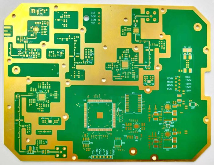
PCB ENIG Cost Calculation: Exact Gold Cost & Total Expense per Square Meter
I. Core Assumptions for PCB ENIG Cost Calculation (Industry Standards)
PCB Specification: 1 square meter double-sided board (standard size for consumer electronics, industrial control, and other applications)
Gold-Plated Area Pricing Rule: PCB manufacturers set a minimum billing ratio of 20% (i.e., if the gold-plated area accounts for ≤20% of the total area of both PCB sides, it is billed at 20%; for ratios exceeding 20%, pricing is adjusted proportionally). This article uses the 20% threshold for calculation.
Gold Thickness: 2 microinches (2μin), equivalent to 0.0508μm (conversion basis: 1 microinch = 0.0254μm). This thickness meets the IPC-4552 Class 2 standard, balancing performance and cost efficiency.
Gold Density: Industry standard value of 19,300 kg/m³ (19.3 g/cm³), using industrial-grade gold with a purity of ≥99.9%.
Current Gold Price: 1,000 CNY/g (market reference price in January 2026, subject to fluctuations driven by global economic conditions and geopolitical factors).
Exchange Rate: 1 CNY ≈ 0.1427 USD (central parity rate announced by the China Foreign Exchange Trade System on January 15, 2026).
Processing Fee Standard: 90 CNY/m² (covering gold salt conversion, nickel plating underlayer, process handling, etc., excluding pure gold cost).
II. Calculation of Pure Gold Cost for 1 Square Meter ENIG PCB (Step-by-Step Precision)
(1) Core Formulas
(2) Detailed Calculation Process
Actual Gold-Plated Area Calculation: Total PCB area (1 m²) × 20% billing ratio = 0.2 m²
Unit Conversion: Gold thickness 0.0508μm = 0.0508×10⁻⁶ m (ensuring unit consistency for volume calculation)
Gold-Plated Volume Calculation: 0.2 m² × 0.0508×10⁻⁶ m = 1.016×10⁻⁸ m³
Pure Gold Consumption Calculation: 1.016×10⁻⁸ m³ × 19,300,000 g/m³ ≈ 0.196 g (exact value: 0.196088 g)
Pure Gold Cost Calculation:
CNY: 0.196 g × 1,000 CNY/g = 196 CNY/m² (exact value: 196.09 CNY/m²)
USD: 196 CNY × 0.1427 USD/CNY ≈ 27.97 USD/m² (exact value: 27.98 USD/m²)
III. Total ENIG Cost Composition for 1 Square Meter PCB
Pure Gold Cost: 196 CNY/m² (accounting for 68.5% of the total cost)
Processing Cost: 90 CNY/m² (accounting for 31.5% of the total cost), covering:
Gold salt conversion fee (covering material loss and process cost of converting gold into ENIG solution; notably, gold-to-gold-salt conversion and ENIG plating involve highly toxic chemicals, requiring strict internal and external management protocols throughout production, transportation, processing, and storage, with substantial associated management costs incorporated in this fee item)
Nickel plating underlayer fee (100 microinch nickel layer to ensure gold layer adhesion and corrosion resistance)
Pre-treatment and post-treatment fees (copper surface cleaning, coating inspection, ion cleaning, etc.)
Equipment depreciation and environmental compliance costs (RoHS compliance testing, wastewater treatment, etc.)
Total Cost Summary
CNY: 196 CNY/m² + 90 CNY/m² = 286 CNY/m²
USD: 27.97 USD/m² + (90 × 0.1427) USD/m² ≈ 27.97 + 12.84 = 40.81 USD/m²
IV. Industry Insights & Key Considerations
Impact of Thickness on Cost: For every 0.025μm increase in gold thickness, the pure gold cost rises by approximately 49 CNY/m² (based on current gold prices). However, the thickness should be controlled within the 0.05–0.1μm range; excessive thickness may cause solder joint embrittlement, while insufficient thickness increases the risk of black pad defects.
Gold Price Volatility Risk: In 2026, global gold prices are poised to rise further, driven by Federal Reserve monetary policies and geopolitical tensions. PCB manufacturers are advised to lock in costs through long-term procurement agreements or hedging strategies.
Avoiding Area Pricing Disputes: When cooperating with PCB manufacturers, clarify the gold-plated area measurement standard (calculated based on solder mask opening area) to prevent cost disputes caused by inconsistent pricing methods.
Alternative Process Comparison: For cost-sensitive projects, a hybrid process of Organic Solderability Preservative (OSP) + selective ENIG can reduce overall costs by 15%–20% without compromising core performance.
V. Frequently Asked Questions (FAQ)
Q1: Is the 20% minimum billing ratio for gold-plated area a universal industry standard?
Q2: Why does pure gold cost account for such a large proportion of total ENIG costs?
Q3: How to verify if the gold layer thickness provided by the manufacturer meets the standard?
Q4: Is there a significant cost difference between ENIG and electroplated gold processes?
Q5: Is there room for negotiating ENIG processing fees when purchasing PCBs in bulk?
VI. Core Keywords
PCB ENIG Cost
Circuit Board Gold Plating Pricing
PCB Surface Finish Cost
ENIG Process Expense
PCB Pure Gold Cost
Conclusion
- long board pcb
- Flexible PCBs
- Special PCB
- Express Printed Circuit Board
- Pcb Prototype
- LED PCB
- PCB
- Printed Circuit Board
- Pcb meaning
- Pcb manufacturer
- Rigid pcb board
- Rigid Flex PCB

 Quote
Quote
 E-mail