PCB Design is the cornerstone of modern electronics, enabling the development of devices from simple gadgets to complex machinery. Mastering PCB design requires a blend of technical knowledge, creativity, and precision. This guide delves into the essentials, providing insights to help professionals and enthusiasts refine their skills and achieve exceptional results.
What is PCB Design?
PCB design involves creating a layout for a printed circuit board that connects electronic components through conductive pathways, pads, and other features. The design is critical to ensuring the device’s functionality, reliability, and manufacturability.
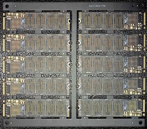
PCB Design
Key Components of PCB Design
- Schematic Design
- The initial step where the electronic circuit is mapped out using specialized software.
- Purpose: Defines how components like resistors, capacitors, and ICs interact.
- PCB Layout
- Involves placing components and routing electrical connections on a virtual board.
- Goal: Optimize space, minimize noise, and ensure efficient signal flow.
- Layers
- PCBs can have single, double, or multiple layers.
- Impact: Increases complexity and functionality for advanced designs.
- Design Rules and Constraints
- Includes guidelines for trace width, spacing, and component placement.
- Importance: Ensures manufacturability and prevents electrical issues.
- Gerber Files
- The final output of the design process, used for manufacturing the PCB.
Tools and Software for PCB Design
- Eagle: Ideal for beginners and professionals.
- Altium Designer: Comprehensive features for advanced users.
- KiCad: Free and open-source, suitable for various projects.
- OrCAD: Robust capabilities for complex PCB systems.
Steps to Master PCB Design
1. Understand the Basics
- Familiarize yourself with the key electronic components such as resistors, capacitors, diodes, and ICs.
- Study fundamental circuit theory, including current flow, voltage drops, and signal integrity principles.
- Research and adhere to industry standards like IPC guidelines to ensure your designs meet quality and safety requirements.
- Learn the different types of PCBs, such as single-layer, multilayer, and rigid-flex PCBs, to choose the right one for your project.
2. Use the Right Software
- Select PCB design software that fits your skill level, such as KiCad, Eagle, or Altium Designer.
- Explore software-specific features like auto-routing, 3D visualization, and simulation tools.
- Take online courses or tutorials to master advanced functions like differential pair routing and impedance control.
- Set up design libraries for components to streamline future projects and maintain consistency.
3. Plan Your Design
- Start by drafting a comprehensive schematic, ensuring clarity in connections and labeling.
- Decide the number of layers based on circuit complexity and signal routing needs.
- Optimize the PCB’s size to balance functionality and cost, considering manufacturing constraints.
- Plan for thermal management by placing heatsinks, vias, or copper pours for heat dissipation.
- Include test points to facilitate troubleshooting and debugging during development.
4. Component Placement
- Prioritize placing components like microcontrollers, connectors, and power regulators first, ensuring proper orientation and accessibility.
- Group related components to shorten traces and improve signal flow.
- Avoid placing components too close to the board edges or near high-heat areas.
- Ensure adequate spacing between components for assembly and maintenance purposes.
- Use the grid system in your software to align components neatly.
5. Optimize Trace Routing
- For high-frequency signals, use controlled-impedance traces and keep trace lengths uniform.
- Separate analog and digital signals to minimize interference.
- Use copper pours for ground planes to improve signal integrity and reduce noise.
- Avoid acute angles in traces; use smooth bends to reduce electromagnetic interference (EMI).
- Consider trace width and spacing to handle current capacity and prevent short circuits.
6. Ensure Power and Ground Integrity
- Design robust power distribution networks (PDNs) with decoupling capacitors near ICs.
- Use wide traces or planes for power and ground to minimize voltage drops and resistance.
- Plan for star grounding or dedicated ground layers to prevent ground loops.
7. Run Design Rule Checks (DRC)
- Use your design software’s DRC feature to verify trace width, spacing, and other parameters meet manufacturing specifications.
- Check for potential short circuits, unconnected nets, or overlapping pads.
- Validate impedance control and ensure layer stack-up alignment matches the board’s design.
8. Add Silkscreen and Labels
- Include clear silkscreen labels for component identifiers, test points, and orientation markers.
- Add your company logo, project name, or version number for identification.
- Ensure the silkscreen doesn’t overlap with solder pads or obstruct vias.
9. Test and Validate
- Create a prototype using a quick-turn PCB manufacturing service.
- Test the prototype under real-world operating conditions to verify functionality and reliability.
- Use tools like oscilloscopes and multimeters to check signal integrity and power distribution.
- Gather feedback from the testing phase and refine your design to address any issues.
10. Prepare for Manufacturing
- Generate Gerber files, bill of materials (BOM), and assembly drawings using your design software.
- Verify file formats meet the requirements of your chosen PCB manufacturer.
- Consider panelizing your design if multiple boards are needed, optimizing manufacturing efficiency.
- Communicate with the manufacturer to confirm design specifications, materials, and timelines.
11. Iterate and Improve
- Learn from each design and manufacturing process to refine your skills.
- Stay updated with industry trends and emerging technologies to enhance your PCB designs.
- Experiment with advanced concepts like flexible PCBs, embedded components, or high-speed designs for specialized applications.
Common Challenges in PCB Design
- Signal Integrity Issues
- Poor routing can lead to interference and signal loss.
- Thermal Management
- Improper heat dissipation can damage components.
- Power Distribution
- Ensure stable power supply across the board to prevent voltage drops.
- Design for Manufacturability (DFM)
- Failing to consider production constraints can increase costs and errors.
Advanced Techniques
- High-Speed Design
- Manage impedance, reflections, and timing for high-frequency signals.
- Flexible and Rigid-Flex PCBs
- Incorporate flexible materials for wearable and compact devices.
- 3D Modeling
- Use 3D software to visualize the PCB in its final enclosure.
- EMI/EMC Mitigation
- Design strategies to minimize electromagnetic interference.
The Future of PCB Design
- AI and Machine Learning: Automating design optimization.
- IoT and Miniaturization: Pushing boundaries of size and complexity.
- Eco-Friendly Practices: Focus on sustainable materials and processes.
Conclusion
Mastering PCB design is a journey of continuous learning and adaptation to evolving technologies. By understanding the fundamentals, leveraging advanced tools, and refining your techniques, you can create innovative and efficient designs that drive progress in electronics.
Whether you’re a novice or an expert, embracing these principles will help you excel in the art of PCB design.
Also can check it on linkedin linkedin sqpcb.com

- long board pcb
- Flexible PCBs
- Special PCB
- Express Printed Circuit Board
- Pcb Prototype
- LED PCB
- PCB
- Printed Circuit Board
- Pcb meaning
- Pcb manufacturer
- Rigid pcb board
- Rigid Flex PCB
 Quote
Quote
 E-mail