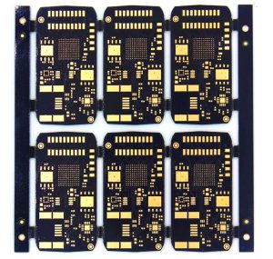
PCB Board Production: Printed Circuit Boards (PCBs) are the foundation of modern electronics. Every device you interact with, from smartphones to industrial machinery, relies on the precise production of PCB boards to function seamlessly. PCB board production is not just about creating physical components; it’s a sophisticated process that transforms innovative designs into high-performing realities. This guide explores the journey from PCB design to final production, covering every essential aspect along the way, from PCB manufacturing and fabrication to thermal management in PCBs and PCB production trends.
PCB Board Production
The Basics of PCB Board Design
Understanding the Role of PCB Boards in Electronics
PCB boards connect and support electronic components, forming the backbone of all electronic devices. These boards ensure functionality, manage electrical currents, and optimize performance.
Key Components of a PCB Board Design
- Substrate Material: Provides structural integrity and is crucial in PCB material selection.
- Copper Layers: Conduct electrical signals.
- Solder Mask: Protects copper traces from oxidation.
- Silkscreen: Adds labels for assembly.
How Design Decisions Impact Production Efficiency
Decisions on layout, trace width, and material selection can affect PCB production cost and timelines. Simplifying the design reduces complexity and potential errors during manufacturing.
Tools and Software for PCB Board Design
Top PCB Design Software for Beginners and Professionals
- KiCad: Open-source and versatile.
- Altium Designer: Advanced features for professionals and supports PCB stack-up design.
- Eagle: Intuitive for small to medium projects.
Creating PCB Schematics: Best Practices for Success
Start with a clear schematic that defines component connections. Use standardized symbols and logical layouts to ensure accuracy.
Optimizing PCB Layouts for Performance and Cost
Efficient layouts reduce signal interference and manufacturing waste. Compact designs save material costs while maintaining performance, especially in custom PCB production.
Preparing for PCB Production
From Concept to Blueprint: Transforming Designs into Gerber Files
Gerber file generation is essential for translating designs into a format manufacturers can use. These files detail every layer of the PCB for accurate production.
Choosing the Right Substrate: FR4, Ceramic, Aluminum, and More
- FR4: Most commonly used, cost-effective.
- Ceramic: Excellent for high-frequency PCB production.
- Aluminum: Ideal for thermal management in PCBs, particularly in flexible PCB manufacturing.
Key Considerations for PCB Stack-Up Design
Proper stack-up minimizes crosstalk and improves signal integrity, especially in multilayer PCB production for advanced applications.
The PCB Manufacturing Process Explained
Etching Copper Layers: Creating Conductive Pathways
Chemical etching removes excess copper, leaving precise conductive pathways that connect components. This is a critical step in PCB fabrication.
Drilling and Plating Holes: From Through-Holes to Vias
Drilled holes and vias provide connectivity between layers, essential for double-sided and multilayer PCBs.
Applying Surface Finishes: HASL, ENIG, and OSP Compared
Surface finishes for PCBs protect copper traces and improve solderability:
- HASL: Affordable and reliable.
- ENIG: Flat finish, ideal for fine-pitch components.
- OSP: Eco-friendly and cost-effective.
Advanced Techniques in PCB Board Production
Multilayer PCB Manufacturing for High-Performance Applications
Multilayer PCB production involves stacking multiple copper layers, enabling compact designs and high functionality in telecommunications and computing.
Flexible PCB Manufacturing and Rigid PCB Production
- Flexible PCBs: Bendable for wearable tech and compact devices.
- Rigid PCBs: Durable for traditional high-performance PCB solutions.
Incorporating Thermal Management Features Like Heat Sinks
Thermal vias and copper pours enhance heat dissipation, critical for high-frequency PCB production and devices with significant power demands.
Quality Control in PCB Production
Essential Testing Methods: Flying Probe, In-Circuit Testing, and More
- Flying Probe Testing: Checks connectivity without a custom fixture.
- In-Circuit Testing (ICT): Validates component functionality.
- Automated Optical Inspection (AOI): Detects physical defects like misalignment.
Ensuring Signal Integrity and Electrical Conductivity
PCB testing methods ensure the board meets electrical performance standards, vital for avoiding signal loss and interference.
The Role of Automated Testing in Mass Production
Automation speeds up testing processes, ensuring consistent quality for PCB scaling in mass production.
Managing Costs in PCB Board Production
Factors That Affect PCB Production Costs
- Material type and thickness.
- Number of layers and vias.
- Surface finish choice and design complexity.
How to Reduce Costs Without Compromising Quality
- Use standard materials and components.
- Optimize design for manufacturability.
- Order in bulk to benefit from volume discounts.
The Benefits of Bulk Production and Panelization
Panelization reduces material waste and production time by grouping multiple PCBs on a single panel, enhancing overall PCB production cost efficiency.
Common Challenges in PCB Board Production
Dealing with Design-to-Production Discrepancies
Misaligned expectations between designers and manufacturers can lead to delays and errors, particularly in custom PCB production.
Managing Thermal and Electrical Constraints
Proper planning mitigates overheating and signal interference, especially in high-density interconnect (HDI PCB production).
Ensuring Consistency in Large-Scale Manufacturing
Consistency is achieved through stringent quality control measures and adherence to PCB production standards.
Industry Trends in PCB Board Production
Eco-Friendly PCB Manufacturing Practices
Sustainable practices, such as recycling materials and using eco-friendly finishes, are becoming industry standards.
The Rise of Smart PCBs for IoT Applications
Smart PCBs integrate sensors and wireless modules, driving innovation in IoT devices.
Innovations in Advanced PCB Production Techniques
HDI PCB production and flexible PCB manufacturing are reshaping the future of electronics with compact, high-performance designs.
Applications of PCB Boards Across Industries
Automotive: Powering Advanced Driver Assistance Systems (ADAS)
PCBs manage critical systems like braking, navigation, and infotainment in modern vehicles.
Medical Devices: Precision PCBs for Life-Saving Equipment
Medical-grade PCBs ensure reliability in devices like pacemakers and diagnostic machines.
Telecommunications: High-Speed PCBs for 5G Networks
PCBs enable faster data transfer and connectivity, essential for advancing telecommunications.
The Future of PCB Board Production
How AI and Automation Are Revolutionizing PCB Manufacturing
AI-driven tools optimize designs and streamline production, reducing errors and improving efficiency.
The Role of 3D Printing in Rapid Prototyping
3D printing enables faster iteration and testing of PCB designs, cutting development timelines significantly.
Emerging Materials and Their Impact on PCB Performance
Innovations in materials like graphene and advanced ceramics promise enhanced conductivity and heat resistance.
Conclusion
PCB board production is a complex yet fascinating process that transforms innovative designs into functional realities. From PCB prototyping and advanced manufacturing techniques to eco-friendly PCB production, every step ensures quality, reliability, and performance. As technology advances, PCB production continues to evolve, driving innovation across industries and paving the way for smarter, more efficient devices.
linkedin https://www.linkedin.com/feed/update/urn:li:activity:
7097167729337532416/

- long board pcb
- Flexible PCBs
- Special PCB
- Express Printed Circuit Board
- Pcb Prototype
- LED PCB
- PCB
- Printed Circuit Board
- Pcb meaning
- Pcb manufacturer
- Rigid pcb board
- Rigid Flex PCB
 Quote
Quote
 E-mail