How PCB Board Printing Brings Your Electronic Ideas to Life
Imagine holding an idea so powerful it could revolutionize an industry. Maybe it’s a groundbreaking medical device, a cutting-edge wearable, or a high-speed communication system. The blueprint is in your mind, the design on your computer, but how do you bring it to life? Enter PCB board printing—the unsung hero that transforms your electronic concepts into tangible, functional realities. Without it, even the most brilliant innovations remain trapped in the digital realm.
PCB board printing is more than a manufacturing process; it’s the lifeblood of modern technology. Every smartphone, drone, and medical sensor owes its existence to this intricate craft. It’s a precise combination of art and engineering, where every layer, trace, and component placement matters. If you’ve ever wondered how your electronic ideas leap from design to reality, it’s time to dive into the fascinating world of PCB board printing.

What is PCB Board Printing? The Core of Electronic Innovation
At its essence, PCB board printing is the process of fabricating printed circuit boards that connect and power electronic components. Think of it as constructing the highway system of your electronic project. It enables signals to flow seamlessly, ensuring every component works in harmony. Without PCBs, even the simplest devices would be a tangled mess of wires and chaos.
The magic of PCB printing lies in its ability to take complex designs and make them manufacturable, scalable, and precise. Whether it’s a single-layer board for a basic gadget or a multi-layer masterpiece for an aerospace application, the process ensures every electronic idea has a solid foundation.
Step-by-Step: How PCB Board Printing Works
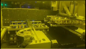
1. PCB Boards Manufacturing: Cutting the Raw Material
The manufacturing process begins with cutting the raw PCB material. The material, typically fiberglass-reinforced copper foil, is cut to the required size. The accuracy of cutting is critical, with a tolerance of +/-2mm. Common material sheet sizes include 36”*48”, 40”*48”, and 42”*48”. Material utilization is important for reducing waste, and in special cases, materials can be mixed for cutting to optimize production efficiency.

2. PCB Boards Manufacturing: Inner Layer Processing
This stage involves several sub-processes:
Pre-treatment: Cleaning and preparing the laminate to ensure a contaminant-free surface.
Coating: Applying a photosensitive coating on the laminate surface.
Exposure: Using a photomask to expose the coating to UV light, transferring the design pattern onto the laminate.
Development and Etching: Developing the exposed pattern and removing unwanted copper using a chemical etching solution.
Drilling: Drilling holes for vias and component leads.
AOI (Automated Optical Inspection): Conducting visual inspection to ensure quality.
At SQPCB, advanced techniques such as LDI (Laser Direct Imaging) exposure machines and fully automated coating and baking lines are used. The use of LDI technology minimizes film shrinkage issues, ensuring precise alignment and reducing registration errors. This innovation helps maintain controlled shrinkage within 0.1um, improving the overall quality of the inner layers.

3. Lamination and Pressing
The lamination process involves the bonding of multiple layers to create multi-layer PCBs. This step includes:
Brown-Out and Riveting: Pre-pressing the laminate to form a stable base.
Pre-Stacking: Aligning the stacked layers of copper, laminate, and prepregs.
Pressing: Applying heat and pressure to bond the layers together.
X-ray Drilling Targets: Drilling targets are aligned and inspected using X-ray systems.
Edge Trimming and Grinding: Trimming the edges and ensuring uniformity in thickness.
Pressing is one of the most critical steps in multi-layer PCB production. SQPCB has optimized this process by selecting structures that not only meet the required board thickness but also improve impedance control. Materials such as 7628 are selected over more expensive options like 2116, significantly reducing costs while ensuring high performance.
4. Drilling Process
Drilling is a crucial step for creating holes for vias and through-hole components. It involves:
Pre-Drilling: Initial drilling to prepare the material for deeper cuts.
Drill Bit Grinding: Ensuring the drill bits are sharpened to maintain precision.
Pinning and Drilling: Ensuring accurate hole placement and depth.
Drill Bit Retirement and Peak Polishing: Polishing drill bits after 3,000-5,000 holes to maintain their effectiveness.
SQPCB uses linear motor-driven drilling machines, ensuring high-speed and high-precision drilling. These machines guarantee hole accuracy and consistency, ensuring that all holes meet IPC standards with a tolerance of +/-2mil.

5. Electroplating Process
Electroplating is essential for copper deposition inside drilled holes and on the PCB surface. The process includes:
High-pressure Water Washing: Ensuring the board is clean before electroplating.
PTH (Plated Through-Hole): Plating copper inside the holes for electrical conductivity.
Copper Electroplating: Depositing a thin layer of copper onto the surface and inside the holes to ensure good electrical connections.
SQPCB uses renowned electroplating equipment, investing in high-quality systems that improve yield and reduce the failure rate. While equipment costs may be higher, the long-term benefits of reduced downtime and superior quality outweigh the initial investment.

6. Outer Layer Processing
After the inner layers are completed, the outer layer processing begins. It includes:
Pre-treatment: Cleaning the copper surface before applying the protective coatings.
Film Lamination: Applying a protective film for further processing.
Exposure and Development: Using LDI technology to transfer the design onto the outer layer.
Etching and Removal: Removing the unwanted copper, leaving behind the designed circuit pattern.
AOI and Impedance Testing: Ensuring the design meets the required impedance and quality standards.
At SQPCB, LDI exposure machines with linear motor and optical scale control help achieve shrinkage accuracy within 0.1um, ensuring excellent alignment and reducing defects caused by manual handling.

7. Solder Mask Application
A solder mask is applied to the PCB to protect copper traces and prevent solder bridges during the assembly process. The steps include:
Pre-treatment and Silk Printing: Printing the solder mask onto the PCB.
Pre-baking: Pre-curing the solder mask to harden it before exposure.
Exposure and Development: Using UV light to expose and harden the mask where needed.
SQPCB implements automated solder mask applications, significantly reducing manual errors such as solder mask shift or incorrect pad coverage. This system helps maintain uniformity and ensures a high-quality finish for all PCBs.
8. Text and Legend Printing
Text and legends are applied to the PCB to mark components, references, and other essential information. The process includes:
Silk Screen and Inkjet Printing: Printing labels and other markings.
Post-Baking: Curing the printed ink to ensure durability.
SQPCB uses linear motor-driven inkjet printing machines, achieving exceptional control over shrinkage and print accuracy. This technology reduces defects caused by misalignment and guarantees clear, legible text.

9. Surface Finishing
A surface finish is applied to exposed copper areas to protect against oxidation and improve solderability. This step includes:
Gold Immersion (ENIG), HASL, or OSP: The choice of surface finish is based on customer requirements for durability and solderability.
")
10. Final Inspection and Electrical Testing
Before assembly, PCBs undergo a series of tests to ensure their functionality:
Electrical Testing: Detects open circuits, short circuits, or misalignments.
Flying Probe Testing and AOI: Ensure the PCB meets design specifications.
Final inspection is essential to ensure that no defects are present and the PCBs meet industry standards before packaging.

Why PCB Board Printing is Essential for Innovation
PCB board printing isn’t just a technical process—it’s the bridge between imagination and implementation. Here’s why it’s indispensable:
1. Prototyping for Perfection
Before mass production, prototypes are essential for testing. They allow engineers to validate their designs, identify flaws, and optimize performance. Rapid prototyping services make this step faster than ever, helping innovators stay ahead in competitive markets.
2. Enabling Advanced Technologies
From 5G networks to autonomous vehicles, today’s cutting-edge technologies demand high-performance PCBs. With specialized materials and intricate designs, PCB printing enables these advancements to become reality.
3. Cost-Effective Manufacturing
Efficient PCB printing processes reduce waste and streamline production. By testing and refining designs during prototyping, companies can avoid costly errors in full-scale manufacturing.
Challenges in PCB Printing and How to Overcome Them
Despite its importance, PCB printing isn’t without its challenges. Common hurdles include:
Design Errors: Misplaced traces or insufficient spacing can lead to malfunctions. Meticulous design checks and simulations can prevent this.
Material Compatibility: Selecting the wrong substrate can compromise performance. Always consider the environmental and electrical demands of your project.
Manufacturing Defects: Even small errors in production can render a board unusable. Partnering with experienced manufacturers ensures higher quality.
Tips for Successful PCB Board Printing
Invest in Quality Design Software: Accurate designs lead to better boards. Tools like Altium Designer or KiCAD can help.
Test, Test, Test: Never skip the prototyping phase. Real-world testing reveals issues that simulations can’t.
Work with Reputable Manufacturers: Experience and expertise matter. Choose a manufacturer with a proven track record and advanced capabilities.
Conclusion: From Concept to Creation
PCB board printing is the heartbeat of modern electronics. It takes your vision from a digital schematic to a tangible, functional device. Whether you’re creating a prototype for the next big thing or scaling up for production, the process ensures that your ideas come to life with precision and reliability.
Embrace the power of PCB board printing and watch as your electronic innovations move from concept to creation. With the right design, materials, and manufacturing partner, the possibilities are endless.
linkedin sqpcb.com

- long board pcb
- Flexible PCBs
- Special PCB
- Express Printed Circuit Board
- Pcb Prototype
- LED PCB
- PCB
- Printed Circuit Board
- Pcb meaning
- Pcb manufacturer
- Rigid pcb board
- Rigid Flex PCB
 Quote
Quote
 E-mail