Printed Circuit Boards (PCBs) are integral to modern electronics, providing a structured platform for connecting components to create functional circuits. The journey from design to finished PCB is detailed and involves numerous precision-driven steps to ensure each board is high-quality, reliable, and optimized for performance. Here’s a closer look at each stage in the PCB manufacturing process, from initial design to final testing.
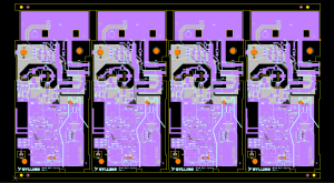
PCB board Manufacturing Process
Step 1: PCB board Manufacturing Process , Design and Layout Preparation
The PCB journey starts with a precise design. Engineers utilize specialized software tools such as Altium, Eagle, or KiCAD to create a digital layout. This design dictates the component placement, copper pathways, and overall structure of the board.
- Schematic Creation: This provides a map of all connections in the circuit.
- Design Rule Check (DRC): A check to ensure the layout meets the manufacturing standards and guidelines.
The design is then exported as Gerber files, which are industry-standard files manufacturers use to guide the process.
Step 2: PCB board Manufacturing Process Imprinting the Circuit Pattern on the PCB
The digital design is transferred onto the copper-clad board surface.
- Photoresist Application: A photosensitive film (photoresist) is applied to the copper layer.
- Exposure and Development: UV light exposes the pattern from the photomask, hardening the areas intended to remain, while unexposed areas are removed, revealing the circuit pattern.
Step 3: PCB board Manufacturing Process Etching Excess Copper
Etching removes the unwanted copper, leaving only the necessary conductive paths.
- Chemical Etching: A solution, often ferric chloride or similar, dissolves unwanted copper.
- Inspection: This step checks that only the essential copper remains on the board.
Step 4: PCB Manufacturing Process Layer Alignment and Bonding (For Multilayer PCBs)
For multilayer boards, multiple copper layers are accurately aligned and laminated together.
- Layer Alignment: Registration pins align each layer perfectly.
- Lamination: Layers are heat-pressed to bond securely, forming a single board structure.
Step 5: PCB Manufacturing Process Drilling Holes
Precise holes are drilled for component leads, mounting, and inter-layer connectivity.
- CNC Drilling Machines: Computerized drilling machines create exact holes based on the design files.
- Verification: Hole alignment and sizing are checked for accuracy.
Step 6: PCB Manufacturing Process Copper Plating and Deposition
To connect layers, copper plating is applied within the drilled holes.
- Electroless Copper Plating: The board is submerged in a solution that deposits a thin copper layer in the holes.
- Electroplating: An electric current is applied to reinforce the copper layer, enhancing connectivity.
Step 7: PCB Manufacturing Process Solder Mask Application
Solder mask covers the board, protecting copper traces and preventing solder bridges.
- Application: An epoxy-based layer is applied, typically green, covering the board.
- Exposure and Development: UV light exposes only necessary areas, leaving solder pads and holes uncovered.
Step 8: PCB Manufacturing Process Silkscreening
Text, symbols, and indicators are printed on the PCB to guide component placement.
- Silkscreen Printing: White ink (or another color) is used to print reference marks and other information.
- Curing: The ink is heat-cured to remain intact.
Step 9: PCB Manufacturing Process Surface Finishing
A surface finish is applied to improve the pads’ solderability and protect the copper.
- HASL (Hot Air Solder Leveling): Solder is applied and leveled with hot air.
- ENIG (Electroless Nickel Immersion Gold): Gold plating is added, especially for boards needing high reliability.
Step 10: PCB Manufacturing Process Testing and Quality Checks
Testing ensures the PCB functions correctly and meets quality standards.
- Automated Optical Inspection (AOI): Cameras scan the board for any flaws.
- Electrical Testing: Tests confirm correct electrical connections, with advanced boards undergoing X-ray inspection for further accuracy.
Step 11: PCB Manufacturing Process Board Cutting and Shaping
The PCB is cut to its final dimensions.
- V-Scoring or Routing: Machines cut the board or score it for easy separation.
- Edge Smoothing and Cleaning: Board edges are smoothed, and any debris is removed.
Step 12: PCB Manufacturing Process Final Inspection and Packing
The final inspection ensures each board is defect-free before packaging.
- Inspection: A final check confirms all aspects meet specifications.
- Anti-Static Packaging: Boards are packed to prevent static damage during shipping.
PCB manufacturing is a complex, multi-step process that requires precision and quality control to ensure reliability. Each step, from initial design to final inspection, contributes to the functionality and durability of the PCB, making it a critical part of the electronics industry. By understanding these steps, manufacturers and designers can better appreciate the intricacies involved and the importance of quality assurance throughout the PCB manufacturing process.
linkedin sqpcb.com

- long board pcb
- Flexible PCBs
- Special PCB
- Express Printed Circuit Board
- Pcb Prototype
- LED PCB
- PCB
- Printed Circuit Board
- Pcb meaning
- Pcb manufacturer
- Rigid pcb board
- Rigid Flex PCB
 Quote
Quote
 E-mail