PCB Board Manufacturing: In the intricate world of electronics, the foundation of every modern innovation lies in one essential component: the printed circuit board (PCB). From smartphones to aerospace systems, PCBs are at the heart of every technological breakthrough. But what ensures that these circuit boards function flawlessly under pressure? The answer lies in a reliable production process.
Creating a high-quality PCB isn’t just about assembling components; it’s about precision in every stage of PCB fabrication and PCB assembly. From selecting the right type of board—single-layer PCB, double-layer PCB, or multi-layer PCB—to perfecting the PCB layout and PCB routing, every step matters. Let’s dive deeper into what makes the production process reliable and capable of meeting today’s demanding standards.
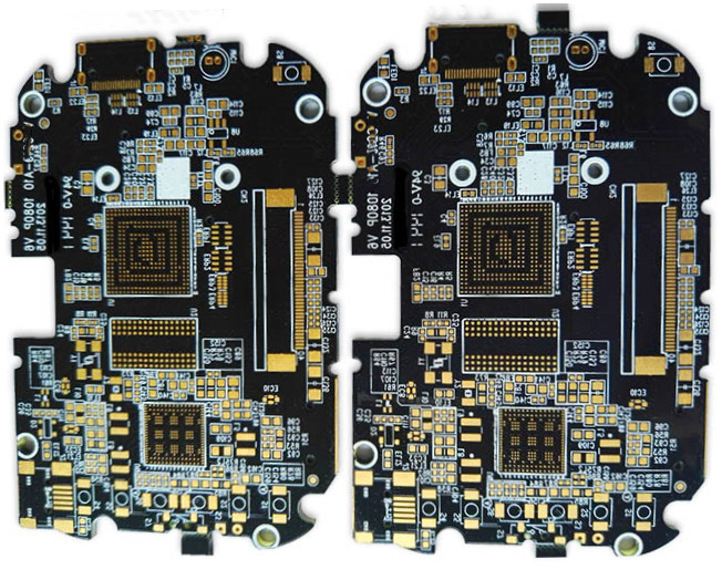
pcb board manufacturing
Understanding PCB Board Manufacturing
What is PCB Manufacturing?
PCB manufacturing is the process of designing, fabricating, and assembling printed circuit boards. These boards serve as the backbone of electronics, allowing components to communicate via conductive pathways, traces, and vias.
A reliable PCB manufacturing process ensures that the PCB stack-up is optimized, the trace width is precise, and the via types are suited to the design’s requirements. It encompasses various types of PCBs, including rigid-flex PCBs, flexible PCBs, high-frequency PCBs, metal core PCBs, and ceramic PCBs, each tailored to specific applications.
The Key to Reliability: A Robust Manufacturing Process
1. Designing the PCB: Precision Starts Here
The journey of a PCB begins with its design. Engineers use advanced tools to create the PCB layout, ensuring that the traces, vias, and components are arranged for maximum efficiency and performance.
- Trace Width and Spacing: Proper trace width ensures the board can handle current without overheating.
- PCB Stack-Up: For multi-layer PCBs, optimizing the stack-up is essential to balance signal integrity and thermal performance.
- Via Types: Depending on the design, different vias—through-hole, blind, or buried—are used to connect layers or route signals effectively.
2. Selecting the Right PCB Type
Choosing the correct PCB type is critical to reliability and performance:
- Single-Layer PCBs: Simplest design, ideal for low-complexity devices.
- Double-Layer PCBs: Provide more connectivity and versatility for moderately complex designs.
- Multi-Layer PCBs: Perfect for high-density designs requiring compactness, such as advanced computing or telecommunications.
- Flexible PCBs and Rigid-Flex PCBs: Used in applications like medical devices or wearables that demand adaptability and durability.
- High-Frequency PCBs: Essential for RF and microwave applications requiring minimal signal loss.
- Metal Core PCBs: Designed for high-heat environments, such as LED lighting and automotive systems.
- Ceramic PCBs: Offer superior thermal conductivity and reliability for aerospace and military applications.
3. Fabrication: Bringing the Design to Life
Substrate Preparation and Circuit Patterning
The PCB fabrication process begins with preparing the substrate. A layer of copper is bonded to the base material, followed by applying a photoresist to create the circuit pattern. This is etched to form the conductive pathways.
- PCB Routing: Ensures optimal signal flow and minimizes interference.
- HDI PCBs: Use advanced techniques like microvias and laser drilling for compact designs with high connectivity.
Layer Lamination for Multi-Layer Boards
For multi-layer PCBs, layers are carefully aligned and bonded under heat and pressure. The PCB stack-up is meticulously planned to enhance performance and reliability.
4. Drilling and Plating
Drilling is performed to create holes for component leads and vias. The holes are plated with conductive material to establish connections between layers.
- Via Types:
- Through-Hole Vias: Extend through the entire board.
- Blind Vias: Connect external layers to internal layers.
- Buried Vias: Connect internal layers without appearing on the surface.
5. Solder Mask and Silkscreen Application
The solder mask is applied to protect the copper traces and prevent short circuits during PCB assembly. A silkscreen layer is added for labeling components, ensuring accurate placement.
6. Quality Control and Testing
Reliability in PCB manufacturing is achieved through rigorous quality control:
- Electrical Testing: Ensures all circuits are properly connected.
- Automated Optical Inspection (AOI): Detects defects in traces, vias, and solder mask.
- Functional Testing: Simulates real-world conditions to verify performance.
Why Reliability Matters in PCB Manufacturing
A reliable PCB manufacturing process ensures:
- Durability: Prevents failures in demanding environments.
- Performance: Optimizes signal integrity and thermal management.
- Scalability: Accommodates both small prototypes and high-volume production.
Conclusion
From designing the perfect PCB layout to ensuring precision in PCB fabrication and PCB assembly, a reliable manufacturing process is the backbone of high-quality PCBs. By selecting the right type—be it a single-layer PCB, rigid-flex PCB, or high-frequency PCB—and focusing on meticulous execution, you can create boards that deliver exceptional performance and durability.
Investing in a robust production process isn’t just about meeting current needs; it’s about building a foundation for innovation and success. With the right PCB manufacturing process, your designs won’t just function—they’ll excel.
linkedin sqpcb.com

- long board pcb
- Flexible PCBs
- Special PCB
- Express Printed Circuit Board
- Pcb Prototype
- LED PCB
- PCB
- Printed Circuit Board
- Pcb meaning
- Pcb manufacturer
- Rigid pcb board
- Rigid Flex PCB
 Quote
Quote
 E-mail