Introduction
Printed Circuit Boards (PCBs) are the silent enablers of modern electronics, shaping the way signals, power, and data are transferred within compact devices. With the rapid push toward high-density interconnect (HDI) fabrication, the industry demands technologies that not only provide finer resolution but also deliver consistency, reliability, and scalability. Among these technologies, PCB Alkaline Etching stands out as a cornerstone for precision engineering.
PCB Alkaline Etching is more than just a chemical removal process; it is a carefully controlled mechanism that defines conductor geometries, stabilizes impedance, and directly influences signal integrity. In the context of HDI fabrication, where microvias, fine lines, and ultra-thin copper layers are the norm, the role of etching expands beyond traditional subtractive manufacturing. It becomes a strategic enabler for achieving design miniaturization without compromising electrical performance.
In this article, we will explore the science, applications, and future of PCB Alkaline Etching. The discussion will extend from fundamental chemistry to industrial practices, followed by an in-depth evaluation of its impact on product reliability.
PCB Alkaline Etching
Fundamentals of PCB Alkaline Etching
1. Understanding PCB Alkaline Etching
At its core, PCB Alkaline Etching is a subtractive process in which unwanted copper is chemically dissolved from a PCB surface using an alkaline solution, typically based on ammoniacal compounds. Unlike acid-based etching, alkaline chemistry offers enhanced control over etching directionality, producing cleaner sidewalls and more uniform conductor widths.
The key components of the process include:
-
Copper-clad laminate: The base substrate covered with copper.
-
Photoresist mask: Protects regions of copper that should remain as conductors.
-
Alkaline etchant: Commonly ammonium hydroxide with additives to control dissolution rate.
-
Etching equipment: Spraying or immersion systems designed for uniform solution delivery.
When copper interacts with ammoniacal etchants, it forms soluble copper-ammonia complexes. The removal rate can be precisely tuned by adjusting pH, temperature, and solution flow dynamics. This level of controllability is what makes PCB Alkaline Etching ideal for HDI applications, where line/space dimensions often shrink below 50 microns.
My perspective: The elegance of PCB Alkaline Etching lies in its balance between chemistry and engineering. It is not only about dissolving copper but also about orchestrating a uniform process across large production panels, something that directly translates into manufacturing yield.
2. Historical Evolution of PCB Alkaline Etching in HDI Manufacturing
The adoption of PCB Alkaline Etching dates back several decades, originally introduced to replace less predictable acid-based methods. In the early years of PCB fabrication, acid etching dominated due to its simplicity. However, as devices demanded finer line definition, the shortcomings of acid etchants—such as undercutting and rough sidewalls—became evident.
By the 1980s and 1990s, alkaline systems emerged as the preferred method for advanced PCB production. With the rise of HDI circuits, where line widths dropped significantly, alkaline chemistry proved to be not just advantageous but essential. Modern formulations integrate inhibitors, stabilizers, and advanced monitoring systems, ensuring that the etching rate is both predictable and repeatable.
Today, PCB Alkaline Etching is regarded as a cornerstone of miniaturization technologies, enabling manufacturers to achieve reliable line widths of less than 25 microns in certain cutting-edge facilities.
3. Chemical Principles Behind PCB Alkaline Etching
The science behind PCB Alkaline Etching revolves around ammonia-copper chemistry. The dissolution of copper in an alkaline medium proceeds through the formation of soluble copper-ammonia complexes, primarily [Cu(NH₃)₄]²⁺.
Key aspects of the chemistry include:
-
Oxidation potential: Oxygen dissolved in the etching bath acts as an oxidizing agent, facilitating copper dissolution.
-
pH sensitivity: Maintaining a pH between 8.0 and 9.5 is critical for balancing etch rate and stability.
-
Temperature control: Elevated temperatures (around 45–55°C) accelerate dissolution but must be carefully monitored to prevent over-etching.
-
Additives: Complexing agents and surfactants reduce sidewall roughness and improve uniformity.
From an engineering standpoint, this chemistry allows precise control over etch factor—the ratio of lateral etching (undercut) to vertical etching depth. A lower etch factor translates into straighter sidewalls, which is critical for HDI circuits.
Thoughts: What fascinates me about this process is the marriage between chemistry and physics. Engineers are essentially harnessing chemical kinetics and fluid dynamics to sculpt copper with nanometer-level precision. This fusion of disciplines underscores why PCB Alkaline Etching continues to evolve even today.
4. PCB Alkaline Etching vs. Acid Etching: A Comparative Perspective
While both alkaline and acid etching aim to remove copper selectively, their performance characteristics differ substantially:
| Parameter | Acid Etching | PCB Alkaline Etching |
|---|---|---|
| Sidewall quality | Prone to undercutting | Straighter sidewalls |
| Resolution | Limited for fine lines | Excellent for microcircuits |
| Cost | Lower initial cost | Higher, but justified by yield |
| Environmental impact | Corrosive, challenging disposal | Easier to recycle copper complexes |
| Suitability for HDI | Poor | Ideal |
Acid etching still finds use in simple, low-density PCBs, where the demand for precision is not critical. However, when it comes to smartphones, wearables, automotive sensors, and aerospace modules, PCB Alkaline Etching is the undisputed choice.
Process Mechanics of PCB Alkaline Etching
5. PCB Alkaline Etching in Copper Removal
At its most fundamental level, copper removal is the essence of PCB Alkaline Etching. Yet, what seems like a straightforward subtractive process is, in reality, a delicate balance of chemistry, mechanics, and control systems.
When the PCB panel enters the etching line, jets of alkaline solution are sprayed over the exposed copper surfaces not protected by photoresist. These jets must maintain uniform distribution, ensuring that every square centimeter of the panel is etched consistently. The dynamic flow prevents localized stagnation, which could otherwise lead to uneven copper removal and defects.
A critical engineering factor is etch uniformity across large panels. With PCB sizes scaling up to accommodate multiple circuit images, controlling edge-to-center etch rate variations becomes a top priority. Engineers often employ real-time monitoring systems, measuring copper concentration and adjusting the chemistry accordingly.
My insight: The act of copper removal may sound destructive, but in practice, it is constructive precision. Instead of merely erasing material, the process is actively shaping conductive paths that define device intelligence.
6. Controlling Line Widths with PCB Alkaline Etching
One of the defining features of HDI fabrication is the ability to achieve fine line widths and spacing. With PCB Alkaline Etching, this control is possible through precise tuning of the etching parameters.
-
Etch factor management: By maintaining an optimal ratio between vertical and lateral etching, engineers ensure conductor walls remain straight. A poor etch factor results in undercutting, which can distort line geometry and compromise impedance control.
-
Spray nozzle design: Uniform jet pressure and distribution directly affect how evenly copper is dissolved across the board. Advanced multi-nozzle arrays are engineered to minimize micro-turbulence while ensuring complete chemical coverage.
-
Process feedback systems: Optical inspection and AI-driven analytics are increasingly employed to compare etched results against design intent, enabling real-time corrective actions.
For HDI circuits with 20 µm lines and spaces, PCB Alkaline Etching stands as the most reliable technique available. It not only creates fine geometries but also ensures reproducibility, which is vital when producing thousands of panels for consumer electronics.
Reflection: From my perspective, controlling line widths is where PCB Alkaline Etching truly demonstrates its engineering sophistication. This step translates chemical dissolution into functional electrical highways of modern devices.
7. PCB Alkaline Etching and Surface Uniformity
Beyond line width control, surface uniformity is a hidden but critical aspect of PCB Alkaline Etching. Surface roughness and irregularities may not be visible to the naked eye, but at gigahertz frequencies, they directly affect signal loss and impedance stability.
Key factors influencing surface uniformity include:
-
Etchant flow dynamics: Proper circulation avoids micro-pitting and localized over-etching.
-
Temperature homogeneity: Thermal gradients in the bath can create inconsistent etch depths across the panel.
-
Photoresist adhesion: Imperfect masking can cause resist lifting, leading to over-etched zones.
Modern etching lines deploy closed-loop process control systems with temperature sensors, pressure regulators, and even machine learning algorithms that predict where uniformity issues might occur. The result is copper traces with minimal roughness, ideal for high-frequency PCBs used in 5G and radar applications.
My view: Surface uniformity is often underappreciated because it lacks dramatic visibility. However, in the real world, it is the difference between a PCB that simply functions and one that enables cutting-edge communication technologies.
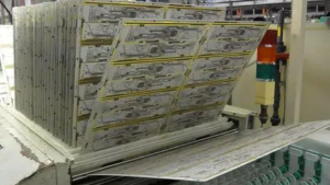
8. Equipment and Automation in PCB Alkaline Etching
The machinery behind PCB Alkaline Etching has evolved significantly. Traditional immersion tanks have largely been replaced by automated spray etching systems, where panels pass through carefully engineered chambers.
Modern equipment incorporates:
-
Spray chamber zoning: Panels move through multiple zones, each with controlled chemistry, spray angles, and flow rates.
-
Automated chemical replenishment: Sensors measure copper ion concentration, automatically dosing fresh etchant or oxidizers to maintain stability.
-
Robotic handling: Automated loaders and conveyors reduce manual handling, ensuring cleanroom-compatible processing.
-
AI-driven predictive maintenance: Equipment now integrates predictive algorithms that flag nozzle clogging, pump wear, or solution imbalance before they cause downtime.
In high-volume HDI fabrication, such automation ensures scalability without compromising precision.
PCB Alkaline Etching in High-Density Interconnect Fabrication
9. Why PCB Alkaline Etching Matters for HDI Circuits
High-Density Interconnect (HDI) technology has become the backbone of modern electronics, from smartphones and tablets to high-performance computing and aerospace systems. HDI is characterized by microvias, fine traces, and reduced layer counts, all designed to enable smaller form factors while increasing functional density.
In such designs, even micron-level deviations in conductor definition can lead to severe consequences such as impedance mismatches, crosstalk, or outright circuit failure. This is where PCB Alkaline Etching demonstrates its critical value.
Key contributions of PCB Alkaline Etching in HDI include:
-
Precision in trace definition: Essential for achieving 20 μm or even smaller line/space configurations.
-
Compatibility with stacked microvias: Ensuring interconnections between multiple layers are reliable.
-
Enhanced electrical consistency: Maintaining uniform impedance across high-speed transmission lines.
My perspective: I see PCB Alkaline Etching as more than just a process—it is an enabler of miniaturization. Without it, the scaling trends in consumer and industrial electronics would stall, limiting innovation in areas such as 5G, IoT, and AI hardware.
10. PCB Alkaline Etching and Microvia Definition
Microvias—tiny holes with diameters as small as 50 μm—are a defining feature of HDI boards. They provide interconnections between layers, enabling compact layouts. However, for microvias to function effectively, the copper traces leading to them must be precisely aligned and cleanly defined.
PCB Alkaline Etching supports this requirement by:
-
Creating sharp trace edges: Ensuring accurate registration between vias and pads.
-
Preventing undercutting near via pads: Avoiding weakening of copper around microvia entry points.
-
Enabling stacked and staggered vias: Which demand ultra-clean geometries for reliability under repeated thermal cycles.
The industry has seen clear evidence that poorly controlled etching results in misalignment or weakened interconnects, which can fail under thermal or mechanical stress. By contrast, alkaline etching delivers the stability needed for multilayer HDI systems.
Reflection: To me, the beauty of this lies in the fact that microvias—tiny structures invisible to the naked eye—can determine the success or failure of billion-dollar product ecosystems. And at the center of this lies the invisible precision of PCB Alkaline Etching.
11. PCB Alkaline Etching for Fine Line Resolution
Fine line resolution is arguably the most critical differentiator in HDI technology. As devices require higher I/O density, designers reduce trace widths and spacing to below 30 μm. Achieving this consistently across large production runs is no trivial task.
PCB Alkaline Etching enables fine resolution through:
-
Controlled anisotropy: Maintaining vertical sidewalls reduces trace narrowing.
-
Uniform spray distribution: Prevents “over-etched” zones that would break fine lines.
-
Optimized chemistry: Use of stabilizers reduces microscopic roughness that could disrupt high-frequency signals.
For example, in 5G antenna modules, signal paths must be tightly controlled. Even a deviation of a few microns can distort performance. PCB Alkaline Etching ensures that the fabricated structures mirror the CAD design, preserving performance integrity.
My thought: Fine line resolution is where science and art intersect. The science lies in chemical kinetics; the art lies in tuning conditions so that thousands of lines on a panel remain consistent without deviation.
12. Yield Improvement through PCB Alkaline Etching
In manufacturing, yield is everything. A process that delivers precision but only on half the panels is commercially unsustainable. This is why yield improvement is a key argument for PCB Alkaline Etching in HDI production.
How it drives yield:
-
Reduced defect rates: Fewer instances of open circuits or shorts caused by over-etching.
-
Repeatability across panels: Stable chemistry ensures that the first panel and the thousandth look the same.
-
Minimized scrap: Lower rework costs and reduced material wastage.
Manufacturers adopting advanced alkaline etching lines have reported yield improvements of 5–12% compared with acid-based processes, which, at industrial scale, translates into millions of dollars saved annually.
Performance Benefits of PCB Alkaline Etching
13. PCB Alkaline Etching and Electrical Performance
Electrical performance is a non-negotiable parameter in modern PCB design. Signal integrity, impedance control, and crosstalk reduction are all directly tied to how accurately copper traces are defined during fabrication.
PCB Alkaline Etching plays a crucial role in this by:
-
Defining uniform conductor widths: Preventing impedance mismatches across differential pairs.
-
Reducing surface roughness: Lower roughness minimizes conductor losses at GHz frequencies, critical for 5G and high-speed computing.
-
Maintaining tight tolerances: Deviations as small as ±2 μm can make or break a high-frequency channel, and alkaline etching ensures tighter distribution.
For instance, in data center PCBs, high-speed SerDes channels rely on line geometries etched with near-perfect accuracy. Any inconsistency can increase bit error rates and compromise system throughput.
My reflection: In the digital age, speed is everything. But speed is meaningless without reliability. PCB Alkaline Etching silently supports the global digital economy by ensuring that billions of signals per second travel without distortion.
14. PCB Alkaline Etching for Reliability and Durability
Reliability in PCBs is not just about function—it’s about longevity under stress. Devices today are expected to endure thermal cycles, mechanical vibration, and exposure to varied environments.
PCB Alkaline Etching enhances reliability in several ways:
-
Straight sidewalls: Reduce the risk of “weak spots” that can delaminate or crack.
-
Consistent trace geometry: Ensures even current distribution, lowering hot-spot formation.
-
Reduced undercutting: Strengthens copper adhesion to the substrate, enhancing mechanical robustness.
In industries such as aerospace and automotive, reliability standards are unforgiving. A small defect in trace geometry can lead to catastrophic failures. By ensuring stable process outputs, alkaline etching directly supports compliance with IPC Class 3 and MIL-SPEC standards.
My thought: When I think of reliability, I picture a satellite orbiting Earth or a self-driving car navigating traffic. In both cases, failure is not an option, and that is precisely where PCB Alkaline Etching earns its place as an enabler of mission-critical reliability.
15. PCB Alkaline Etching and Thermal Management
Thermal performance is a growing concern as devices become more powerful yet smaller. Heat concentration on PCBs can degrade components, shift impedance, and shorten device lifespan.
PCB Alkaline Etching indirectly contributes to better thermal management by:
-
Maintaining uniform copper thickness: Prevents localized hot spots from uneven conductor widths.
-
Enabling fine-line routing: Which supports better current distribution across layers, reducing thermal stress.
-
Facilitating integration with thermal vias: Cleaner via-to-trace connections improve heat transfer efficiency.
For high-power LED drivers and electric vehicle inverters, where PCBs act as both electrical and thermal conduits, etching precision ensures that heat dissipation pathways remain effective throughout the product’s lifecycle.
Reflection: In my view, thermal management has shifted from being an afterthought to being a primary design driver. PCB Alkaline Etching plays an invisible but vital role in enabling systems to stay cool, safe, and reliable.
16. Environmental Advantages of PCB Alkaline Etching
In addition to performance benefits, environmental sustainability has become a defining metric in manufacturing. Acid-based etching processes are notoriously challenging in waste treatment due to their corrosiveness and higher toxicity. By contrast, PCB Alkaline Etching offers more manageable environmental profiles.
Key advantages include:
-
Recyclability of copper: Dissolved copper forms soluble complexes that can be recovered and reused.
-
Lower chemical aggressiveness: Compared to strong acids, alkaline solutions are easier to neutralize and dispose of.
-
Reduced worker hazards: Improved safety profiles for operators handling etching systems.
Forward-looking PCB manufacturers have started integrating closed-loop chemical recovery systems, where copper recovered from alkaline etching is reintroduced into production as raw material. This circular approach not only reduces environmental impact but also lowers material costs.
Conclusion
PCB Alkaline Etching is more than a manufacturing step—it is a cornerstone technology in the evolution of modern electronics. From defining ultra-fine traces in high-density interconnect (HDI) boards to enabling the reliability of RF and 5G circuits, alkaline etching has proven itself as a precision-driven, sustainable, and scalable solution.
Frequently Asked Questions (FAQ)
FAQ 1: What is the difference between rolled copper foil and electrolytic copper foil?
Rolled copper foil is produced by mechanically rolling copper into thin sheets, which gives it superior ductility, smooth surface quality, and mechanical strength. This makes it suitable for flexible PCBs and applications that require bending or repeated motion.
Electrolytic copper foil, by contrast, is created via electro-deposition in a chemical bath. It has a grainy surface structure, is more cost-effective, and provides excellent adhesion to substrates, making it popular for rigid PCBs.
FAQ 2: Why is PCB Alkaline Etching preferred over acidic etching in HDI fabrication?
PCB Alkaline Etching is preferred because:
-
It delivers straighter sidewalls with less undercutting.
-
It achieves better line definition, crucial for high-density interconnects.
-
It is more environmentally friendly, allowing efficient copper recovery.
-
It is compatible with automation and fine-pitch designs.
FAQ 3: How does PCB Alkaline Etching impact signal integrity in high-frequency PCBs?
In high-frequency PCBs (5G, RF, and microwave boards), signal integrity depends heavily on trace geometry and surface smoothness.
PCB Alkaline Etching improves performance by:
-
Ensuring uniform trace widths for consistent impedance.
-
Producing clean, smooth copper surfaces that reduce signal scattering.
-
Minimizing etch-related roughness, which can otherwise cause high-frequency losses.
FAQ 4: Is PCB Alkaline Etching environmentally sustainable?
Yes, compared to traditional acidic etching, PCB Alkaline Etching is more sustainable:
-
Copper recovery systems allow dissolved copper to be recycled into usable metal.
-
Lower ammonia formulations reduce emissions and environmental impact.
-
Closed-loop rinse systems minimize water waste.
FAQ 5: What future innovations can we expect in PCB Alkaline Etching?
The future will likely bring:
-
Sub-10 μm line/space capability for next-generation HDI.
-
AI-driven etching control with predictive defect prevention.
-
Hybrid PCB-semiconductor substrates for advanced packaging.
-
Zero-waste facilities with full copper recycling.
-
Sustainability certification as a selling point in global markets.

- long board pcb
- Flexible PCBs
- Special PCB
- Express Printed Circuit Board
- Pcb Prototype
- LED PCB
- PCB
- Printed Circuit Board
- Pcb meaning
- Pcb manufacturer
- Rigid pcb board
- Rigid Flex PCB
 Quote
Quote
 E-mail