The evolution of electronics demands innovative solutions that push the boundaries of performance and efficiency. At the heart of this revolution lies multilayer Printed Circuit Board (PCB), which offer unparalleled versatility and functionality. These advanced PCBs are essential for prototyping, enabling the development of cutting-edge devices across industries like telecommunications, automotive, healthcare, and consumer electronics.
Multilayer Printed Circuit Board
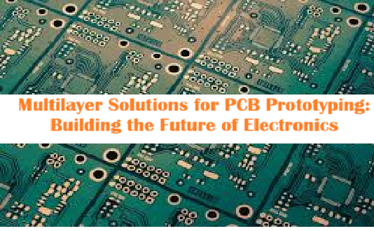
A Multilayer PCB consists of three or more PCB layers of conductive material, separated by insulating substrates and bonded together into a single compact board. This structure enables the creation of high-density PCBs, making them ideal for applications requiring advanced functionality and compact designs.
Structure of a Multilayer PCB
Multilayer PCBs are built with alternating layers of copper and insulating materials. Key elements include:
- Conductive Layers: These carry signals and power, critical for maintaining signal integrity in high-frequency PCBs.
- Insulation (Dielectric) Layers: Provide electrical isolation between conductive layers.
- Power and Ground Planes: Enhance performance by reducing noise and improving impedance control.
- Vias and Microvias: These interconnect the layers, an essential feature of HDI technology for compact designs.
The PCB stack-up is meticulously planned to balance performance, reliability, and multilayer board thickness to suit the application.
Why Choose Multilayer PCBs for Prototyping?
Prototyping with multilayer PCBs is vital for projects requiring advanced designs and high-performance capabilities. Here’s why they are the go-to solution:
1. Compact Design
By stacking multiple layers, multilayer PCB advantages include the ability to reduce the overall size of electronic devices. This is particularly beneficial for consumer electronics PCBs like smartphones and wearables.
2. Enhanced Performance
Multilayer PCBs improve performance by integrating impedance control and dedicated power and ground planes, reducing noise and signal interference. This is especially valuable for telecommunications PCBs used in high-speed signal processing.
3. Increased Durability
The lamination process during PCB fabrication strengthens the board, making it more robust and suitable for demanding environments, such as automotive PCBs.
4. Versatility
Whether it’s for flexible PCBs, rigid-flex PCBs, or high-frequency PCBs, multilayer PCBs support a wide range of applications with their adaptability to complex requirements.
Applications of Multilayer PCB Prototyping
Multilayer PCBs are indispensable in prototyping for a variety of advanced applications:
1. Consumer Electronics
Devices like smartphones, tablets, and wearable technology rely on high-density PCBs for their compact size and advanced functionality.
2. Automotive
Applications such as Advanced Driver-Assistance Systems (ADAS), navigation systems, and electric vehicle (EV) power management depend on reliable automotive PCBs.
3. Healthcare
Medical imaging devices, patient monitoring systems, and portable diagnostic equipment benefit from the precision and reliability of medical PCBs.
4. Telecommunications
5G network equipment and high-frequency signal processing systems require telecommunications PCBs for their ability to handle complex circuits and high-speed signals.
Benefits of Multilayer Solutions in Prototyping
1. Optimized Space Utilization
Multilayer PCBs allow designers to create compact prototypes without sacrificing functionality, making them ideal for space-constrained applications in consumer electronics and healthcare.
2. Improved Signal Integrity
With dedicated ground planes and shorter signal paths, multilayer PCBs minimize electromagnetic interference (EMI) and cross-talk, ensuring reliable signal transmission.
3. Faster Development Cycles
Advanced PCB manufacturing techniques enable prototypes to closely simulate final product performance, accelerating the testing and refinement stages.
Challenges and Solutions in Multilayer Prototyping
1. Complex Design Processes
The design of multilayer PCBs involves intricate layouts and interconnections. Utilizing advanced design software and optimizing the PCB stack-up are critical steps to simplify the process.
2. Thermal Management
Effective heat dissipation is essential for high-density PCBs. Solutions include adding thermal vias, using heat sinks, and selecting high-grade materials during PCB material selection.
3. Manufacturing Precision
The precision required in PCB fabrication is critical for ensuring the alignment and connectivity of layers. Collaborating with experienced manufacturers helps achieve this.
The Role of PCB Manufacturers in Multilayer Prototyping
Reliable PCB manufacturers play a pivotal role in the success of multilayer PCB prototyping. Their expertise ensures that designs are transformed into functional prototypes with precision and efficiency.
1. Custom Prototyping
Manufacturers offer tailored solutions for specific industry requirements, whether for telecommunications PCBs or medical PCBs.
2. State-of-the-Art Equipment
Advanced manufacturing facilities ensure that even the most complex designs, including rigid-flex PCBs, are produced with accuracy.
3. Comprehensive Testing
Rigorous PCB testing methods validate reliability and functionality, ensuring flawless operation in prototypes and final products.
Advanced Features and Innovations in Multilayer PCBs
1. Flexible and Rigid-Flex PCBs
Combining flexibility and durability, these designs are ideal for wearable devices and automotive applications.
2. HDI Technology
HDI technology enables finer traces and microvias, supporting high-speed, high-density designs crucial for compact electronics.
3. High-Frequency and High-Speed Applications
Advanced materials and optimized PCB stack-ups ensure superior performance in high-frequency PCBs.
How to Manage PCB Prototyping Costs
1. Efficient Material Selection
Choose cost-effective materials like FR4 for general applications, and invest in premium materials only when necessary.
2. Optimize Design for Manufacturing
Minimize layer counts and streamline designs to reduce production expenses while maintaining quality.
3. Small-Batch Production
Utilize small-batch PCB production for prototyping to manage costs while testing designs effectively.
Conclusion
Multilayer PCBs are shaping the future of electronics by enabling compact, high-performance prototypes. Their integration into prototyping processes is essential for creating innovative, competitive products across industries. Leveraging the expertise of skilled PCB manufacturers and employing advanced techniques ensures a seamless journey from design to production, empowering designers to turn groundbreaking concepts into reality.
Investing in multilayer PCB prototyping positions your projects for success in an increasingly competitive market, setting the stage for the next wave of technological innovation.
linkedin https://www.linkedin.com/feed/update/urn:li:activity:
7097167729337532416/

- long board pcb
- Flexible PCBs
- Special PCB
- Express Printed Circuit Board
- Pcb Prototype
- LED PCB
- PCB
- Printed Circuit Board
- Pcb meaning
- Pcb manufacturer
- Rigid pcb board
- Rigid Flex PCB
 Quote
Quote
 E-mail