-->
Module PCB: Understanding Modular Printed Circuit Boards
2025-02-16

Module PCB: Types, Applications, Design and Manufacturing Guide

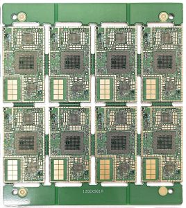
A module PCB is a compact circuit board designed to perform a specific function within a larger electronic system.

Common examples include:

  • Wi-Fi and Bluetooth modules
  • Power supply modules
  • Sensor modules
  • RF communication modules
  • Microcontroller modules
  • Motor control modules
  • Display modules
  • GPS and positioning modules

Instead of designing every function directly onto one large PCB, engineers can divide the system into smaller functional modules.

This modular approach can simplify product development, testing, maintenance, and future upgrades.

From a PCB manufacturing perspective, module PCBs are often relatively small but may require dense routing, controlled impedance, fine-pitch components, thermal management, and reliable board-to-board connections.

Common Types of Module PCB

Common Types of Module PCB


What Is a Module PCB?

A module PCB is a printed circuit board designed around one main function.

For example, an electronic product may contain:

Main Control PCB

Power Module

Wireless Module

Sensor Module

Display Module

Each module performs a specific task and communicates with the main system through:

  • Board-to-board connectors
  • Pin headers
  • FPC connectors
  • Cables
  • Soldered pads
  • Edge connectors

Some modules are supplied as complete PCB assemblies with components already installed, while others may be custom bare PCBs manufactured for later assembly.

Therefore, the term module PCB can describe both the circuit board itself and, in many practical applications, the assembled functional module.


Common Types of Module PCB

1. Wireless Communication Module PCB

Wireless modules provide communication functions such as:

  • Wi-Fi
  • Bluetooth
  • Zigbee
  • LoRa
  • Cellular communication

These PCBs may contain:

  • RF ICs
  • Antennas
  • Filters
  • Matching networks
  • Shielding structures

Important PCB requirements often include:

  • Controlled impedance
  • Stable ground planes
  • Short RF signal paths
  • Stitching vias
  • Low-loss PCB materials when required

2. Power Module PCB

Power modules control or convert electrical power.

Examples include:

  • DC-DC converters
  • AC-DC power modules
  • Voltage regulators
  • Power management boards
  • Motor power stages

Important design considerations include:

  • Copper thickness
  • Current carrying capacity
  • Thermal vias
  • Heat spreading
  • Creepage and clearance
  • Component spacing

Power module PCBs may require heavier copper or special thermal designs depending on the current and power level.


3. Sensor Module PCB

Sensor modules collect information from the surrounding environment.

Examples include:

  • Temperature sensors
  • Pressure sensors
  • Motion sensors
  • Humidity sensors
  • Light sensors
  • Gas sensors

Sensor PCB designs often need careful attention to:

  • Noise control
  • Grounding
  • Signal integrity
  • Analog signal routing
  • Environmental protection

4. Microcontroller Module PCB

A microcontroller module integrates a processor and its supporting circuits into one reusable board.

Typical components include:

  • MCU
  • Memory
  • Crystal oscillator
  • Power regulation
  • Communication interface
  • Programming connector

These modules are widely used in:

  • Embedded systems
  • Industrial control
  • IoT products
  • Prototypes
  • Automation equipment

5. RF Module PCB

RF module PCBs are designed for radio-frequency signal processing.

Applications include:

  • Radar
  • RF amplifiers
  • GPS
  • Antenna modules
  • Microwave communication
  • Wireless base stations

RF PCB modules may require materials such as:

  • Rogers RO4350B
  • Rogers RO4003C
  • Other low-loss high-frequency laminates

Manufacturing accuracy becomes especially important because small changes in:

  • Trace width
  • Dielectric thickness
  • Copper thickness
  • Dk
  • Etching

can influence RF performance.


6. Motor Control Module PCB

Motor control modules are common in:

  • Industrial equipment
  • Robotics
  • Automotive systems
  • Electric propulsion
  • Pumps
  • Fans

These PCBs may combine:

  • Control circuits
  • Power devices
  • Current sensing
  • Communication circuits

Manufacturing considerations may include:

  • Heavy copper
  • Thermal management
  • High-current routing
  • Isolation
  • Reliable connector design

Why Use Module PCBs?

Faster Product Development

Using an existing functional module can reduce development time.

Instead of redesigning:

  • RF communication
  • Power conversion
  • Sensor interfaces

from the beginning, engineers can integrate an existing module into the main system.

This can shorten:

  • Design time
  • Prototype cycles
  • Debugging
  • Verification

Easier System Upgrades

A modular architecture makes future product changes easier.

For example:

An existing Bluetooth module can be replaced by a newer wireless module without redesigning the entire main PCB.

This is useful for products requiring:

  • Multiple product versions
  • Technology upgrades
  • Long product life cycles

Simplified Testing

Each functional module can be tested separately before final system integration.

This helps engineers identify whether a problem originates from:

  • Power supply
  • Communication
  • Sensor circuit
  • Main control board

Modular testing can simplify failure analysis.


Easier Maintenance and Replacement

In some industrial products, replacing one module is easier and less expensive than replacing an entire main board.

This can reduce:

  • Maintenance cost
  • Repair time
  • Product downtime

Flexible Product Platforms

One main system can sometimes support several different modules.

For example:

One control board may support:

  • Wi-Fi version
  • Ethernet version
  • Bluetooth version
  • Cellular version

This allows manufacturers to build multiple product models from one common platform.


Module PCB vs Traditional Main PCB

A module PCB and a main PCB serve different roles.

Feature Module PCB Main PCB
Main Purpose Specific function Complete system control
Size Usually smaller Usually larger
Integration Connects to another board/system Hosts multiple functions
Replacement Often easier Usually more complex
Design Focus Specialized function Overall system integration
Typical Example Wi-Fi module Industrial control main board

There is no strict technical rule defining the size of a module PCB.

The key difference is its functional independence within the larger electronic system.


Module PCB Manufacturing Process

The manufacturing process is generally similar to other printed circuit boards, but smaller module PCBs may involve higher component density and tighter tolerances.

1. PCB Design Review

Before manufacturing, the PCB factory reviews:

  • Gerber files
  • Drill files
  • Stack-up
  • Board thickness
  • Copper thickness
  • Impedance requirements
  • Surface finish
  • Special processes

DFM review is especially useful for dense module designs.


2. Material Selection

Common materials include:

FR-4

Used for most general module PCBs.

High-Tg FR-4

Used when improved thermal reliability is required.

Rogers Materials

Used for RF and microwave modules.

Flexible Materials

Used when the module requires bending or compact interconnection.

Material selection should match the actual electrical and thermal requirements rather than simply choosing the most expensive option.


3. Inner Layer Fabrication

For multilayer module PCBs, inner layers are:

  • Imaged
  • Etched
  • Inspected by AOI

The layers are then prepared for lamination.


4. Lamination

Prepreg and core materials are stacked and bonded under controlled heat and pressure.

Lamination quality affects:

  • Final thickness
  • Layer registration
  • Reliability
  • Impedance performance
The Art and Science of Creating Printed Circuit Boards

The Art and Science of Creating Printed Circuit Boards


5. Drilling and Copper Plating

The PCB is drilled to create:

  • Signal vias
  • Ground vias
  • Component holes
  • Mounting holes

The hole walls are plated with copper when electrical connection is required.


6. Outer Layer Imaging and Etching

Circuit patterns are transferred onto the outer copper layers.

Accurate imaging is especially important for:

  • Fine traces
  • BGA areas
  • High-density modules
  • Impedance-controlled circuits

7. Solder Mask and Surface Finish

Typical surface finishes include:

  • HASL
  • ENIG
  • OSP
  • Hard Gold
  • Gold Flash

ENIG is commonly selected for module PCBs with:

  • Fine-pitch components
  • BGA
  • Flat pad requirements

The most suitable surface finish depends on assembly and product requirements.


8. Electrical Testing

Finished bare PCBs are electrically tested to verify:

  • Continuity
  • Isolation
  • Open circuits
  • Short circuits

Depending on quantity, manufacturers may use:

  • Flying probe testing
  • Test fixtures

Important Module PCB Design Considerations

Component Density

Module PCBs are often designed to save space.

This can create:

  • Narrow routing channels
  • Fine-pitch components
  • Dense via structures

Before increasing PCB complexity, engineers should evaluate whether the layout can be optimized through:

  • Component placement
  • Routing changes
  • Smaller packages
  • 0 Ohm jumper resistors
  • Different connector locations

Increasing the layer count should not always be the first solution.


Signal Integrity

High-speed modules may require:

  • Controlled impedance
  • Differential pairs
  • Continuous reference planes
  • Proper ground stitching
  • Short signal paths

The PCB stack-up should be confirmed before manufacturing.


Thermal Management

Compact modules can concentrate heat in a small area.

Common solutions include:

  • Thermal vias
  • Large copper areas
  • Inner copper planes
  • Heat sinks
  • Thicker copper
  • Thermal interface materials

The correct solution depends on actual power dissipation.


Grounding and EMI

Wireless, RF, power, and high-speed modules may require strong ground control.

Design techniques include:

  • Ground planes
  • Ground vias
  • Stitching vias
  • Via fences
  • Shielding cans

A small grounding detail can have a significant impact on final EMC performance.


Connector Design

Module PCBs frequently connect to another PCB.

Common connection methods include:

  • Board-to-board connectors
  • Pin headers
  • FPC connectors
  • Edge connectors
  • Direct soldering

Connector selection should consider:

  • Current
  • Signal speed
  • Mechanical strength
  • Assembly
  • Service requirements

Via Design in Module PCBs

Module PCB designs often contain many different via types.

Common examples include:

Signal Vias

Transfer signals between layers.

Ground Vias

Connect ground planes.

Thermal Vias

Transfer heat from power components.

Stitching Vias

Connect ground or shielding copper areas to improve EMI performance.

Via in Pad

Used in high-density BGA designs when routing space is limited.

For via-in-pad designs, resin filling and copper capping may be required to prevent solder wicking and provide a flat assembly surface.


Module PCB Cost Factors

Module PCB cost depends on more than board size.

A small PCB can sometimes be more expensive than a much larger board if it requires advanced processes.

Major cost drivers include:

  • Layer count
  • Material type
  • Copper thickness
  • Fine line/space
  • Small via diameter
  • HDI structure
  • Controlled impedance
  • Surface finish
  • Resin-filled vias
  • Special testing

For example:

A small 8-layer HDI module may cost significantly more per square meter than a large standard 2-layer FR-4 PCB.

Therefore, cost optimization should focus on manufacturing complexity, not simply reducing board dimensions.


Module PCB Applications

Consumer Electronics

Used in:

  • Smart appliances
  • Wearable devices
  • Audio products
  • Smart home systems

Industrial Electronics

Used in:

  • PLC systems
  • Motor controllers
  • Automation equipment
  • Sensor systems
  • Communication modules

Automotive Electronics

Used in:

  • Radar
  • Communication
  • Sensors
  • Power control
  • ADAS systems

Automotive applications require careful attention to reliability and thermal performance.


Medical Electronics

Module PCBs may be found in:

  • Monitoring equipment
  • Diagnostic systems
  • Portable medical devices
  • Sensor modules

Reliability and traceability are especially important in medical applications.


Communication Equipment

Typical applications include:

  • RF modules
  • Wireless modules
  • Network equipment
  • Base stations
  • Antenna systems

High-frequency applications may require specialized PCB materials and impedance control.


How to Select a Module PCB Manufacturer

A module PCB manufacturer should be able to support both standard PCB processes and the special requirements of compact electronic modules.

Important capabilities include:

  • Multilayer PCB manufacturing
  • Fine-line processing
  • Controlled impedance
  • HDI capability
  • Via plugging
  • Resin-filled vias
  • ENIG and other surface finishes
  • Electrical testing
  • Engineering and DFM support

For high-frequency or power modules, material experience is also important.

A good PCB supplier should not only manufacture the files exactly as received.

When necessary, the supplier should identify potential issues involving:

  • Manufacturability
  • Cost
  • Reliability
  • Stack-up
  • Material selection

before production begins.


Module PCB Manufacturing from a PCB Factory Perspective

From a manufacturing perspective, a module PCB is not necessarily difficult because it is called a “module.”

The real manufacturing difficulty comes from the design itself.

For example:

A simple power module may only require:

  • 2 layers
  • Standard FR-4
  • HASL
  • Large components

while an RF module may require:

  • Rogers material
  • Controlled impedance
  • Fine lines
  • ENIG
  • Via fencing
  • Tight dimensional control

A high-density processor module may require:

  • Multilayer structure
  • BGA
  • HDI
  • Laser microvias
  • Resin filling
  • Copper capping

Therefore, the correct manufacturing solution should always be based on the actual PCB specification.


Conclusion

Module PCBs provide a practical way to divide complex electronic systems into smaller functional building blocks.

They can improve:

  • Development speed
  • Product flexibility
  • Testing efficiency
  • Maintenance
  • System scalability

Common module PCBs include:

  • Wireless modules
  • Power modules
  • Sensor modules
  • Microcontroller modules
  • RF modules
  • Motor control modules

From a PCB manufacturing perspective, the most important factors are not simply the module’s size or function.

The key considerations are:

Material + Layer Count + Signal Requirements + Thermal Requirements + Via Structure + Surface Finish + Manufacturing Capability

A good module PCB should achieve the required performance without introducing unnecessary manufacturing complexity.


Frequently Asked Questions

What is a module PCB?

A module PCB is a circuit board designed to perform a specific function within a larger electronic system, such as wireless communication, power conversion, sensing, or processing.

Is a module PCB the same as a PCBA?

Not exactly. PCB refers to the bare circuit board, while PCBA normally refers to a PCB with components assembled. In practice, many electronic modules are supplied as complete PCB assemblies.

What materials are used for module PCBs?

Standard FR-4 is the most common. High-Tg FR-4, Rogers high-frequency materials, and flexible materials may be used depending on thermal, RF, or mechanical requirements.

Are module PCBs usually multilayer?

Not always. Simple modules may use 2-layer PCBs, while complex wireless, processor, HDI, or RF modules may require multilayer structures.

Why are module PCBs sometimes expensive despite their small size?

PCB cost is strongly influenced by manufacturing complexity. Small boards may still require many layers, fine traces, HDI, controlled impedance, expensive materials, or advanced via structures.

Can module PCBs use Rogers material?

Yes. RF and microwave modules commonly use low-loss materials such as Rogers laminates when standard FR-4 cannot meet the electrical performance requirements.

Product Center
Contact Us

Get A Quote

Q5dtzF
Quote
E-mail
info@sqpcb.com
Whatsapp
+86 136 0306 3656