Precision PCB Manufacturing: Preventing Ion Migration with Advanced Technology
In the world of PCB manufacturing, some design rules are born from hard-earned experience rather than just theoretical calculations. One such critical rule is maintaining a minimum 0.4mm hole-to-hole spacing – a specification that separates temporary prototypes from reliable production-ready boards.
Ion Migration: The Hidden Reliability Killer
What is Ion Migration?
Ion migration is a form of electrochemical failure. When a DC voltage gradient exists on a PCB in a humid environment, metal ions (primarily copper ions) slowly migrate through moisture-absorbing dielectric materials. These ions gradually move toward the anode under the influence of the electric field, forming dendritic metal deposits that eventually lead to decreased insulation resistance or even short circuits.
The Dangers of Insufficient Spacing
When hole-to-hole spacing falls below 0.4mm, multiple failure mechanisms can occur:
Accelerated Electrochemical Migration: Moisture and contaminants create conductive paths between closely spaced holes
Micro-short Circuit Formation: These “phantom failures” appear only after extended field use

Ion Migration
Insulation Degradation: Constant electrical stress gradually breaks down the insulation material
Lessons from the Field: Electric Toothbrush Case Study
In an electric toothbrush project we participated in, the client insisted on using 0.3mm hole spacing due to space constraints. Despite our risk warnings, the final product experienced approximately 3% customer complaints and returns after about six months of use.
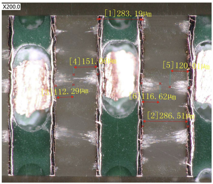
Failure analysis revealed:
In the humid bathroom environment, the tight hole spacing created ideal conditions for ion migration. Copper ions slowly grew under the influence of the electric field, eventually forming conductive channels that led to circuit failure. This case validates the practical value of the 0.4mm safety spacing.
SQPCB’s Engineering-First Approach: Precision Manufacturing Investment
At SQPCB, we understand that preventing such failures requires more than just following specifications – it demands manufacturing excellence. That’s why we’ve made significant investments in advanced equipment that eliminate traditional manufacturing variables:
Precision Manufacturing Infrastructure:
Circuit Pattern LDI Automated Exposure Systems
Eliminates film expansion/contraction issues (traditional films typically have 0.1-0.3% variation)
Ensures perfect alignment regardless of environmental conditions
Maintains consistent line width and spacing control
Solder Mask LDI Automated Exposure Systems
Prevents misalignment and blurring
Ensures perfect solder mask dam definition between fine-pitch components
Guarantees consistent solder mask thickness and coverage
Automated Text Printing Systems
Eliminates manual labeling errors
Provides permanent, legible markings
Maintains positioning accuracy across all boards
Beyond Imaging: Complete Process Control
Our commitment to quality extends throughout the entire manufacturing process:
Own Lamination Process: Complete control over multilayer board reliability
Dedicated Surface Finish Lines (HASL & ENIG): Consistent finish quality and perfect solderability
Reduced Manual Handling: Minimized scratching, contamination, and rework
FAQ Section
Q1: Why is 0.4mm the critical threshold for hole-to-hole spacing?
A1: This threshold is based on extensive field data showing that below this spacing, the risk of electrochemical migration in humid environments increases exponentially. It accounts for material tolerances, manufacturing variations, and real-world environmental factors.
Q2: How does LDI technology specifically prevent alignment issues?
A2: Traditional film-based exposure suffers from thermal expansion/contraction (typically 0.1-0.3%). LDI eliminates this variable by directly imaging from digital data, achieving consistent positioning accuracy within 25μm, regardless of panel size or environmental conditions.
Q3: How long does it typically take for ion migration failures to appear in products?
A3: Based on our experience, ion migration-related failures typically appear 6-18 months after product deployment, depending on environmental humidity, electric field strength, and spacing dimensions. Our electric toothbrush case study began showing failures at approximately 6 months.
Q4: Can you handle boards with even more stringent spacing requirements?
A4: Yes. While we recommend 0.4mm for reliable production, our LDI equipment can consistently maintain 0.3mm spacing where absolutely necessary for high-density designs, with appropriate design validation.
Q5: What are the specific benefits of your in-house lamination and surface finish control?
A5: End-to-end control of these critical processes eliminates communication gaps and quality variations between different suppliers. This translates to better impedance control, more reliable interlayer connections, and consistent surface finish quality – all while reducing lead times by 3-5 days.
Engineering Excellence
At SQPCB, we believe that reliable PCB manufacturing shouldn’t depend on luck or temporary environmental conditions. Our substantial investment in advanced equipment represents our commitment to delivering boards that perform not just on test day, but throughout their entire service life.
- long board pcb
- Flexible PCBs
- Special PCB
- Express Printed Circuit Board
- Pcb Prototype
- LED PCB
- PCB
- Printed Circuit Board
- Pcb meaning
- Pcb manufacturer
- Rigid pcb board
- Rigid Flex PCB

 Quote
Quote
 E-mail