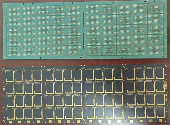
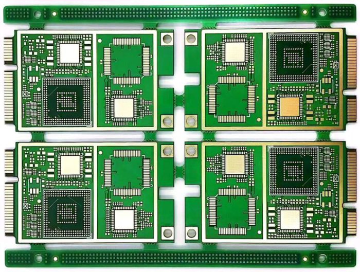
What is an IC Substrate?
IC Substrate (Integrated Circuit Substrate) is primarily used in chip packaging and serves as the “bridge” between the semiconductor chip and the printed circuit board. Chips are extremely small, with pad diameters typically around 0.05 mm, whereas the minimum pad diameter on a standard PCB is usually 0.3 mm or larger. This huge size difference makes it impossible to achieve a reliable direct connection between a chip and a PCB.
To achieve interconnection between the chip and the system circuit, an IC substrate is required as an intermediate carrier. Built on high-performance resin materials, IC substrates feature ultra-fine wiring and microvias. They can enlarge the chip’s tiny pad array into a BGA (Ball Grid Array) structure, making it easier to connect to a PCB. At the same time, IC substrates can also be adapted into other packaging formats such as QFN and CSP, depending on design needs.
In essence, IC substrates act as the chip’s “outer shell” while also serving as the critical bridge for signals and power between the chip and the PCB. This makes them a cornerstone in the semiconductor packaging industry.

What is a PCB?
PCB (Printed Circuit Board) is the fundamental component found in nearly all electronic devices. A PCB achieves electrical interconnection by laying conductive copper traces on an insulating substrate while also providing mechanical support for electronic components.
PCBs come in many types, depending on the application:
Single-layer PCBs: Used in simple devices with only one conductive layer.
Double-layer PCBs: With two conductive layers, connected by vias.
Multilayer PCBs: From 4 layers up to dozens, used in complex electronic systems.
Rigid-flex PCBs: A combination of rigid PCBs and flexible circuits, suitable for compact and foldable applications.
Metal-core PCBs: Such as aluminum PCBs, commonly used in LED lighting and other applications requiring high thermal dissipation.
Compared to IC substrates, PCBs cover a much broader range of applications. From low-cost consumer electronics to aerospace and defense systems requiring extreme reliability, PCBs are indispensable across industries. While PCB manufacturing processes are relatively mature, producing advanced multilayer boards, high-frequency PCBs, and heavy copper boards still demands sophisticated equipment and expertise.

The Difference Between IC Substrates and PCBs
In today’s rapidly growing electronics and semiconductor industry, the importance of circuit substrates has become increasingly evident. From consumer electronics to high-performance computing, from smart cars to 5G communications, every core chip and electronic system relies on two key carriers: IC substrates and PCBs (Printed Circuit Boards).
At first glance, they may look similar since both serve as the foundation for carrying and connecting electronic components. However, their functions, technical requirements, and application scenarios are significantly different. Understanding the distinction between IC substrates and PCBs is crucial for engineers, procurement specialists, and manufacturing companies in the electronics sector.
Key Differences Between IC Substrates and PCBs
| Category | IC Substrate | PCB BOARD |
|---|---|---|
| Primary Use | Semiconductor packaging; connects chip to system circuits | Installs electronic components; forms complete electronic systems |
| Wiring Precision | Line width/spacing < 10 μm | Line width/spacing typically ≥ 50–100 μm |
| Materials | High-performance BT resin, ABF resin; low Dk and low loss | FR4, CEM, metal-core laminates; broad application range |
| Layer Structure | Typically 4–12+ layers for chip packaging | Ranges from single-layer to dozens of layers |
| Manufacturing Process | Advanced LDI exposure, laser drilling, fine copper plating | Mature processes; broad spectrum of complexity |
| Pad Size | Matches chip pad size (~0.05 mm) and converts to BGA or other formats | Smallest pad size typically ~0.3 mm |
| Cost Level | High unit cost; used for advanced semiconductor applications | Wide cost spectrum, from low-cost consumer products to high-reliability systems |
| Industry Positioning | Critical in the semiconductor packaging supply chain | Foundational to the electronics manufacturing supply chain |
From this comparison, it’s clear: IC substrates are the bridge between the chip and the system, while PCBs serve as the foundation for the entire electronic system.
Why Are IC Substrates More Challenging?
Compared with PCBs, IC substrates impose much higher demands on manufacturing:
Extreme alignment precision: With micro-scale wiring, alignment accuracy must be near perfect.
Advanced equipment requirements: Large investments in LDI laser direct imaging, optical alignment systems, and automated inspection equipment are essential.
High yield control: Even the slightest misalignment or defect can cause an entire batch of semiconductor packaging to fail.
Stringent quality standards: IC substrates must comply with semiconductor-grade quality and reliability certifications.
For these reasons, not all PCB manufacturers are capable of producing IC substrates.
SQPCB’s Advantages and Supply Capabilities
As a professional circuit board manufacturer, SQPCB not only produces a wide range of PCBs but also has the capability to supply IC substrates. The company has continuously invested in advanced equipment and upgraded its processes, building strong advantages in high-precision circuit manufacturing.
Key strengths include:
Fully automated LDI exposure lines: Both circuit and solder mask LDI exposure machines ensure high alignment accuracy and stable yields.
Automated legend printing: Eliminates defects associated with traditional screen printing.
In-house lamination and plating processes: Complete control of lamination, copper deposition, HASL, and ENIG, ensuring stability and reliability.
Yield assurance: Optical alignment and automated inspection minimize shrinkage, misregistration, and operator error, guaranteeing accurate solder mask registration for BGA pads.
Material versatility: Beyond FR4, CEM, and aluminum-based PCBs, SQPCB also supplies IC substrates using BT and ABF high-performance resins.
With these capabilities, SQPCB provides customers with end-to-end solutions ranging from standard PCBs to IC substrates, covering industries from consumer electronics and communications to automotive electronics and advanced semiconductor packaging.
Frequently Asked Questions (FAQ)
Q1: What is the main difference between IC substrates and PCBs?
A1: IC substrates are used in semiconductor packaging, bridging chips to system circuits with micro-scale precision, while PCBs are used to assemble electronic components into complete systems.
Q2: Why do IC substrates require such high precision?
A2: Chip pads are only about 0.05 mm in diameter, while the smallest PCB pads are usually 0.3 mm or larger. IC substrates are required to bridge this size gap reliably.
Q3: What materials are typically used for IC substrates?
A3: Common materials include BT resin and ABF resin, both offering low dielectric constant and low signal loss, making them ideal for high-speed and high-frequency applications.
Q4: Can PCBs replace IC substrates?
A4: No. PCBs cannot achieve the micro-scale wiring and high-frequency performance required for chip packaging. IC substrates and PCBs serve different roles and complement each other in the electronics ecosystem.
Q5: Can SQPCB supply both PCBs and IC substrates?
A5: Yes. SQPCB is equipped with advanced LDI exposure machines, in-house lamination and plating lines, and strict quality control, enabling the company to supply both high-quality PCBs and IC substrates for semiconductor and electronics applications.
- long board pcb
- Flexible PCBs
- Special PCB
- Express Printed Circuit Board
- Pcb Prototype
- LED PCB
- PCB
- Printed Circuit Board
- Pcb meaning
- Pcb manufacturer
- Rigid pcb board
- Rigid Flex PCB

 Quote
Quote
 E-mail