IC Substrate vs. Printed Circuit Board (PCB): Key Differences and Applications
With the rapid advancement of semiconductor technology, electronic devices are becoming smaller, faster, and more complex. This has led to the increased demand for both IC substrates and printed circuit boards (PCBs), two essential components in electronic packaging. While they share similarities in structure and function, they serve distinct roles in the electronics industry.
This article explores the differences between IC substrates and PCBs, including their structure, materials, manufacturing processes, applications, and advantages.
Looking for reliable PCB manufacturing or advanced interconnect solutions? SQPCB provides custom high-density PCB and prototype substrate manufacturing, combining speed, precision, and scale.

IC Substrate
1. What is an IC Substrate?
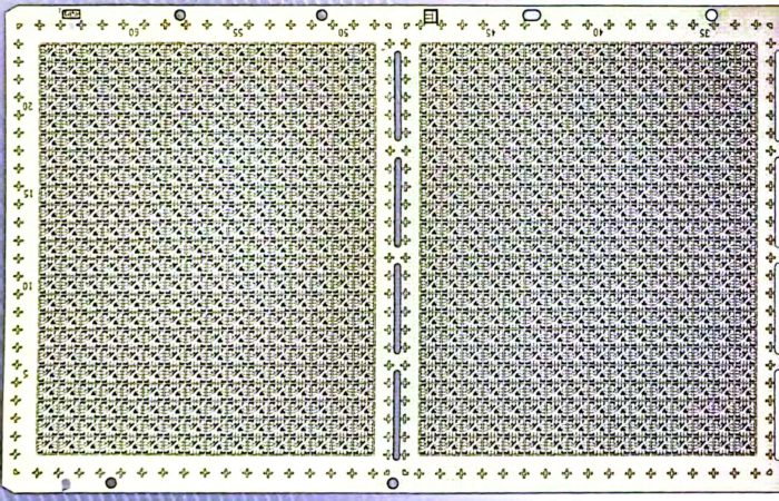
An IC substrate is a type of high-density interconnect (HDI) PCB specifically designed to serve as an intermediary between the semiconductor chip and the main PCB. It provides electrical connections, mechanical support, and thermal management for the integrated circuit (IC).
IC substrates are used in applications such as:
Microprocessors and GPUs
Memory modules (DRAM, NAND Flash, etc.)
System-on-Chip (SoC) and ASIC packaging
High-speed computing and networking devices
Key Features of IC Substrates:
✅ High Density – Ultra-fine traces and microvias for compact, high-performance circuits.
✅ Superior Electrical Performance – Designed to handle high-frequency signals with minimal interference.
✅ Thermal & Mechanical Stability – Uses advanced materials to ensure reliability under extreme conditions.
✅ Precise Manufacturing – Uses complex processes such as substrate-like PCB (SLP) technology and semi-additive processes (SAP) to achieve high precision.

ic substrate
2. What is a Printed Circuit Board (PCB)?
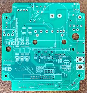
A printed circuit board (PCB) is the foundation of most electronic devices, providing electrical interconnections and mechanical support for components. Unlike IC substrates, PCBs are used at the system level, connecting ICs, resistors, capacitors, and other components to create a functional electronic system.
PCBs are categorized based on their complexity:
Single-layer PCBs – Used in simple electronic devices like LED lighting.
Double-layer PCBs – Common in consumer electronics.
Multilayer PCBs – Used in advanced applications such as computers and telecommunications.
HDI PCBs – Feature microvias and fine-pitch traces for compact devices.
Key Features of PCBs:
✅ Versatile Applications – Used in consumer electronics, automotive, industrial, and medical devices.
✅ Scalability – Available in multiple layers for complex designs.
✅ Variety of Materials – Uses FR4, metal-core, ceramic, and flexible materials based on the application.
✅ Cost-Effective – More economical to produce than IC substrates.

3. IC Substrate vs. PCB: Key Differences
| Aspect | IC Substrate | PCB |
|---|---|---|
| Function | Connects the IC to the main PCB | Connects all electronic components in a system |
| Feature Size | Extremely fine traces (5-15 µm) | Larger traces (50-150 µm) |
| Material | High-performance materials (BT resin, Ajinomoto build-up film) | FR4, metal-core, ceramic |
| Manufacturing Process | Semi-Additive Process (SAP), Embedded Trace Process (ETP) | Subtractive Process (Etching) |
| Applications | CPUs, GPUs, SoCs, high-speed networking devices | Consumer electronics, automotive, industrial control |
| Cost | Expensive due to advanced technology | More cost-effective |
4. Manufacturing Differences Between IC-Substrates and PCBs
4.1 IC-Substrate Manufacturing Process
IC substrates require high-density interconnections, making the semi-additive process (SAP) the preferred manufacturing method.
🔹 Substrate Materials: Uses Ajinomoto build-up film (ABF), BT resin, or polyimide, which offer better thermal and electrical properties than standard PCB materials.
🔹 Fine-Line Manufacturing: Achieves 5-15 µm line/space, much finer than traditional PCBs.
🔹 Advanced Plating Techniques: Uses electroless copper plating and plasma etching to ensure precise trace formation.
🔹 Laser Drilled Microvias: IC substrates feature stacked microvias, ensuring high-density interconnections.
4.2 Manufacturing Process in PCB supplier
PCBs use subtractive etching techniques, where excess copper is removed to create circuits.
🔹 Material Selection: Standard FR4, aluminum-core, ceramic, or polyimide-based materials.
🔹 Layer Stackup: Can be single-layer, double-layer, or multilayer, depending on the complexity.
🔹 Drilling & Plating: Uses mechanical drilling for through-holes and laser drilling for HDI microvias.
🔹 Solder Mask & Surface Finish: Common finishes include ENIG (Electroless Nickel Immersion Gold), HASL, OSP, and immersion silver.
5. Applications of IC Substrates vs. PCBs
| Application | IC-Substrate Usage | PCB Usage |
|---|---|---|
| Consumer Electronics | Found in SoCs and processors for smartphones and tablets | Used in motherboards, power circuits, and displays |
| Automotive Electronics | Used in AI processors and ADAS systems | Found in ECU, infotainment, and power management systems |
| Medical Devices | Essential for compact IC packaging in imaging and diagnostic equipment | Used in PCBs for MRI, ECG, and monitoring systems |
| Telecommunications | Used in high-speed 5G processors and transceivers | Found in base stations, antennas, and routers |
| Computing & AI | Critical for CPUs, GPUs, and AI accelerators | Used in server motherboards, storage devices, and power supplies |
6. Future Trends in IC Substrates and PCBs
6.1 Embedded IC Packaging
IC substrates are moving toward embedding chips within the substrate to reduce signal paths and enhance performance.
6.2 Miniaturization and HDI
Driven by IoT and AI, designs are trending toward finer traces, thinner substrates, and higher layer counts.
6.3 Rise of Substrate-Like PCBs (SLP)
SLP bridges the gap between traditional PCBs and IC substrates. It offers high density at lower costs, suitable for smartphones, AR/VR, and wearables.
7. Conclusion: Which One Do You Need?
🔹 If you are designing IC packaging for high-performance applications like AI, GPUs, or mobile processors, IC substrates are essential for their high density and electrical performance.
🔹 If you need cost-effective interconnections for electronic systems, traditional PCBs are the better choice, as they support a wide range of applications.
For businesses looking for high-quality PCB and IC-substrate solutions, Shenzhen Shuoqiang Electronics offers advanced PCB manufacturing services with precise control over layer count, material selection, and surface finishes to meet your project requirements.
8. Frequently Asked Questions (FAQ)
1. Can IC substrates be used in standard PCB applications?
Not typically. IC substrates are optimized for chip-level packaging, not for general component interconnection.
2. What materials are used in IC-substrates that aren’t in PCBs?
IC substrates use ABF film and BT resin, offering better dielectric and thermal performance than typical FR4.
3. Why is SAP (Semi-Additive Process) important in IC substrates?
SAP allows ultra-fine lines (down to 5 µm) that are critical for modern chip packaging requirements.
4. How does the cost of IC-substrates compare with HDI PCBs?
IC substrates are significantly more expensive due to advanced materials, equipment, and precision requirements.
5. Does SQPCB manufacture both PCBs and IC substrates?
Yes. SQPCB supports both traditional multilayer PCBs and substrate-like PCB solutions, with expertise in fast lead times and precision interconnects.
- long board pcb
- Flexible PCBs
- Special PCB
- Express Printed Circuit Board
- Pcb Prototype
- LED PCB
- PCB
- Printed Circuit Board
- Pcb meaning
- Pcb manufacturer
- Rigid pcb board
- Rigid Flex PCB

 Quote
Quote
 E-mail