High-Speed PCB Manufacturing: Key Considerations and Technologies
High-speed printed circuit boards (PCBs) are fundamental to modern electronics, enabling faster data transmission and reliable performance in a wide range of applications, including telecommunications, computing, automotive, and medical devices. As demand for high-speed data continues to grow, the manufacturing process of these PCBs must evolve to meet the increasingly complex requirements for signal integrity, power distribution, and thermal management. This article explores the technologies and considerations involved in high-speed PCB manufacturing, from design to production.
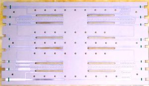
high speed pcb manufacturing
What Makes a PCB “High-Speed”?
A high-speed PCB is designed to handle high-frequency signals with minimal loss, distortion, or interference. These PCBs are used in applications that require fast data transfer and efficient signal processing, such as in servers, networking equipment, smartphones, and advanced computing devices.
Key Characteristics of High-Speed PCBs
High-speed PCBs are engineered with several characteristics to ensure that they can handle high-frequency signals without degrading performance:
- Signal Integrity: The ability to maintain the integrity of high-frequency signals as they travel through the PCB is crucial. This includes minimizing signal loss, reflections, and cross-talk between signal traces.
- Low Loss: Minimizing resistive and capacitive losses in signal paths is essential for ensuring that high-speed signals are transmitted with minimal attenuation.
- Impedance Control: Impedance control ensures that the electrical characteristics of the traces are consistent, helping to avoid reflections and signal distortions.
- Power Integrity: Power distribution networks (PDNs) must be carefully designed to ensure stable power delivery to all components without noise or voltage fluctuations.
Design Considerations for High Speed PCBs
The design of high-speed PCBs requires careful planning to ensure signal integrity, power delivery, and heat management. Several key factors must be considered during the design process.
1. Trace Width and Spacing
The width of traces on a high-speed PCB affects both the impedance and the signal integrity. To ensure consistent impedance, the width of the traces should be carefully calculated based on the PCB material, the trace length, and the required impedance. Similarly, the spacing between traces is critical for preventing cross-talk, which can lead to signal degradation.
2. Material Selection
The choice of PCB material plays a significant role in the performance of high-speed circuits. Materials with low signal loss, such as FR4, Rogers, or Teflon, are commonly used in high-speed PCB manufacturing. These materials help minimize signal degradation and improve performance at high frequencies. Additionally, the dielectric constant (Dk) and loss tangent (Df) of the material must be considered to maintain consistent impedance and minimize signal loss.
- FR4: While it is the most common PCB material, FR4 can have higher losses at very high frequencies, making it less suitable for the most advanced high-speed applications.
- Rogers: A more specialized material, Rogers boards are known for their low loss and stable performance at high frequencies.
- Teflon: Often used in RF and microwave applications, Teflon provides excellent dielectric properties, ensuring minimal signal loss.
3. Impedance Control
Impedance control is a key consideration in high-speed PCB design. Impedance mismatches can lead to signal reflections, which result in data loss and errors. Designers use controlled impedance traces to ensure that the signal integrity is maintained. The impedance of a trace depends on its width, the spacing between the trace and the ground plane, and the type of PCB material.
In high-speed PCBs, differential pairs—two closely spaced traces carrying complementary signals—are often used. These pairs are designed to have matched impedances to minimize reflections and noise. Differential pair routing is crucial in high-speed digital designs, especially for high-frequency signals like those used in PCIe or DDR memory interfaces.
4. Power and Ground Planes
To maintain signal integrity and avoid noise, high-speed PCBs require solid power and ground planes. These planes provide a stable reference for the signals and help minimize voltage fluctuations. Power integrity is critical in high-speed applications, as noise or instability in the power supply can lead to signal distortion.
In some cases, designers will use separate planes for different voltage levels to further reduce noise and maintain stability. In addition, using decoupling capacitors near the power pins of components can help reduce high-frequency noise.
5. Via and Layer Stack-Up Design
The via design and layer stack-up are also important considerations for high-speed PCB manufacturing. Vias can introduce inductance and resistance, which can degrade signal integrity. For high-speed designs, blind and buried vias are often used, as they minimize the impact on the signal path and reduce the total via length.
The layer stack-up design is critical for ensuring proper impedance control, as it determines the arrangement of signal, power, and ground layers within the PCB. A well-designed stack-up ensures that high-speed signals travel with minimal interference from other layers and provides a stable reference plane.
Manufacturing Process for High Speed PCBs
High-speed PCB manufacturing involves several critical steps to ensure that the final product meets the required performance standards. The manufacturing process must be precise, with a focus on ensuring low signal loss, tight impedance control, and minimal interference.
1. PCB Fabrication
The fabrication of high-speed PCBs starts with the preparation of the base material, typically a copper-clad laminate. The material is then drilled, etched, and patterned to create the circuit traces and vias. This process must be done with high precision to ensure the integrity of the traces and the accuracy of the impedance control.
During fabrication, advanced photolithography techniques are used to create fine traces and vias, and laser drills are employed for the accurate placement of vias. A high level of precision is essential to ensure that the traces are properly aligned and that the vias do not interfere with the signal integrity.
2. PCB Assembly
Once the PCB is fabricated, the next step is assembly. Components are placed on the PCB using surface-mount technology (SMT) or through-hole technology (THT). For high-speed applications, SMT is preferred due to its ability to place components with high precision and minimal inductance.
During assembly, careful attention is paid to the placement of components to minimize the length of the signal traces and to ensure that high-speed components are connected efficiently. Additionally, vias should be kept to a minimum, as they can introduce unwanted inductance and signal loss.
3. Testing and Quality Control
Testing is a critical step in ensuring that the high-speed PCB functions as intended. Several types of testing are typically performed:
- Electrical Testing: Ensures that the PCB meets the required electrical specifications and that all connections are intact.
- Impedance Testing: Verifies that the impedance of the traces is within the specified range.
- Thermal Testing: Checks for hot spots and ensures that the PCB can handle the thermal load of high-speed signals.
High-speed PCBs must undergo rigorous quality control checks to ensure that they meet the high standards required for performance. This includes visual inspection, automated optical inspection (AOI), and X-ray inspection for detecting internal defects like voids in the solder joints.
Challenges in High Speed PCB Manufacturing
While high-speed PCB manufacturing has advanced significantly, there are still several challenges that designers and manufacturers must overcome:
- Miniaturization: As devices become smaller and more complex, maintaining signal integrity and power stability becomes more challenging. Smaller form factors require more precise manufacturing techniques and materials.
- Thermal Management: High-speed PCBs often generate significant heat due to the rapid switching of components. Managing this heat is critical to prevent overheating and ensure the longevity of the components.
- Cost: High-speed PCBs typically require more expensive materials and manufacturing processes, which can drive up costs. Balancing performance and cost is always a key challenge in high-speed PCB design.
Future Trends in High Speed PCB Manufacturing
As the demand for faster data transfer and more complex systems grows, the field of high-speed PCB manufacturing continues to evolve. Some of the key trends shaping the future of high speed PCBs include:
- 5G and Beyond: The rollout of 5G networks will drive the need for even faster and more reliable PCBs to support the high-frequency signals required for 5G communications.
- Advanced Materials: Researchers are developing new materials with even lower signal loss and higher thermal conductivity to improve the performance of high-speed PCBs.
- AI and Automation: The integration of artificial intelligence and automation in PCB design and manufacturing will help improve precision, reduce manufacturing time, and enhance quality control.
Conclusion
High-speed PCB manufacturing is a complex process that requires precision, advanced materials, and a deep understanding of electrical and mechanical principles. By focusing on key factors like signal integrity, impedance control, and thermal management, manufacturers can create high-speed PCBs that meet the demanding requirements of modern electronics. As technology continues to advance, the manufacturing of high-speed PCBs will become even more critical, enabling the development of faster, more powerful, and more reliable electronic devices.

- long board pcb
- Flexible PCBs
- Special PCB
- Express Printed Circuit Board
- Pcb Prototype
- LED PCB
- PCB
- Printed Circuit Board
- Pcb meaning
- Pcb manufacturer
- Rigid pcb board
- Rigid Flex PCB
 Quote
Quote
 E-mail