1. Introduction to High Density Interconnect Circuit Boards
High Density Interconnect Circuit Boards (HDI PCBs) have become a pivotal element in the electronics manufacturing industry due to the growing demand for smaller, faster, and more reliable electronic devices. These circuit boards represent the cutting edge of modern electronics and enable the miniaturization of products while simultaneously improving performance.
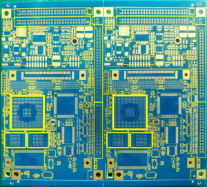
high density interconnect circuit boards
What Are HDI PCBs?
An HDI PCB is a type of printed circuit board (PCB) that utilizes finer lines, microvias, and advanced layering techniques to achieve a high-density configuration. This allows for more components to be integrated into a smaller physical space. Unlike traditional PCBs, HDI PCBs employ multiple layers, which are interconnected by smaller vias that are drilled with precision using advanced laser techniques. These circuit boards are commonly used in applications where performance, miniaturization, and reliability are critical.
The ability to increase the density of interconnects within a given area has revolutionized various industries, including telecommunications, consumer electronics, automotive, aerospace, and medical devices. HDI PCBs not only offer more functionality in less space but also enable devices to operate at higher speeds, with better signal integrity and thermal performance.
Importance of HDI PCBs
As electronic devices become more sophisticated and require greater functionality, the need for HDI PCBs has grown exponentially. From smartphones and laptops to smartwatches and medical devices, HDI PCBs are essential for packing more capabilities into increasingly smaller form factors.
The key advantages of HDI PCBs include:
-
Miniaturization: HDI PCBs allow for more complex circuits to be placed in compact spaces, leading to smaller and lighter electronic devices.
-
Improved Performance: With finer traces, microvias, and optimized signal paths, HDI PCBs help improve the performance of high-speed circuits, reducing noise, interference, and crosstalk.
-
Enhanced Reliability: Due to their robust design and advanced manufacturing techniques, HDI PCBs can withstand extreme environments, making them ideal for use in industries like aerospace and automotive.
-
Cost-Effectiveness: While the initial cost of manufacturing HDI PCBs may be higher, their compactness and performance advantages often lead to cost savings in the long run by reducing the overall size and weight of the device.
In essence, HDI PCBs are a critical enabler of modern electronic devices, allowing manufacturers to meet the growing consumer demand for smaller, faster, and more powerful gadgets.
2. Historical Development of High Density Interconnect Circuit Boards
The development of HDI PCBs is closely tied to the need for more advanced and efficient electronics. The journey of HDI PCBs began in the early days of PCB technology, where simple designs were sufficient for less complex electronics. However, as technology advanced, so did the need for more intricate designs with higher functionality and more components in smaller spaces.
The Early Days of PCB Technology
The first printed circuit boards were simple and used in basic electrical devices in the mid-20th century. These early PCBs were single-layer designs, with copper traces and basic components soldered onto the surface. As electronic devices became more complex, the limitations of single-layer PCBs became apparent. The need for multi-layered PCBs to connect different components in a more compact space arose in the 1960s.
The Emergence of HDI PCBs
In the 1980s, the limitations of traditional PCBs in terms of space and interconnectivity were increasingly felt as consumer electronics and telecommunications systems became more advanced. The trend toward miniaturization of devices required a new approach to PCB design. HDI PCBs emerged as a solution to these challenges.
HDI PCBs were initially adopted in the military and aerospace sectors, where high-performance standards were required. These sectors needed more compact and reliable designs that could handle higher frequencies and thermal stresses. Early HDI designs used advanced technologies such as microvias and laser drilling to achieve higher density interconnections.
The 1990s: Commercialization of HDI PCBs
By the early 1990s, the demand for HDI PCBs had expanded beyond aerospace and defense applications and began to enter the consumer electronics market. The proliferation of mobile phones, portable computers, and other handheld devices created a growing need for small, high-performance PCBs. This shift towards mass-market consumer electronics led to the development of more cost-effective HDI manufacturing processes, making HDI PCBs more accessible to a wider range of industries.
During this period, advancements in materials, such as new laminates and copper foils, further improved the capabilities of HDI PCBs, enabling them to handle higher frequencies and provide greater signal integrity. The 1990s also saw the introduction of automated manufacturing techniques, which significantly improved the efficiency and scalability of HDI PCB production.
The 2000s and Beyond: HDI PCBs in Modern Electronics
The 2000s marked a turning point in the widespread adoption of HDI PCBs across various sectors, including automotive, medical devices, and industrial electronics. With the advent of technologies like smartphones, tablets, and GPS devices, the demand for compact and high-performance circuit boards continued to rise.
Today, HDI PCBs are at the core of many advanced technologies, including wearable devices, drones, and IoT applications. They are crucial for meeting the challenges of ultra-small, high-performance electronic devices that require dense interconnections and high reliability.
The development of 3D circuit board technologies and flexible HDI PCBs further expands the possibilities for future applications, enabling new levels of functionality in even smaller and more flexible packages.
3. Core Technologies in High Density Interconnect Circuit Boards
The development of High Density Interconnect Circuit Boards (HDI PCBs) hinges on several core technologies that make them more efficient and capable of handling high-speed signals, increased component densities, and miniaturization. These technologies enable the construction of PCBs with finer traces, smaller vias, and multiple layers, all while maintaining reliability and performance. Below, we’ll explore some of the key technologies that define HDI PCBs.
3.1 Microvias
One of the foundational technologies that sets HDI PCBs apart from traditional circuit boards is the use of microvias. Microvias are smaller holes that interconnect layers of the PCB, and they can be as small as 75 microns in diameter, making them significantly smaller than the traditional vias used in conventional PCBs.
Microvias enable high-density routing, which allows for more compact designs with fewer layers. They also provide better electrical performance by reducing the path length for signals traveling between layers. This is especially important for high-frequency applications, where longer via paths can cause signal degradation.
Microvias are typically produced using laser drilling, which ensures high precision and enables the creation of vias that are both smaller and more consistent than those produced by mechanical drilling. Laser drilling also allows for blind vias and buried vias, which are key to increasing density while reducing the overall size of the PCB.
3.2 Sequential Lamination
Sequential lamination is a critical technology used in HDI PCBs to enable the construction of multi-layer designs. In traditional PCBs, layers are created simultaneously and then stacked. However, in HDI PCBs, layers are added one by one in a process called sequential lamination. This allows for greater flexibility in the design and ensures that the vias, which connect the layers, can be made smaller and more precise.
Sequential lamination also facilitates the creation of complex layer structures where multiple layers are bonded together to form a multilayer PCB. This technique is widely used to create stacked vias and microvia interconnections, which are essential for achieving the high-density designs that HDI PCBs are known for.
3.3 Fine-Line and Fine-Pitch Technology
Fine-line and fine-pitch technology are essential for achieving the high-density interconnects in HDI PCBs. Fine lines refer to the width of the traces that interconnect components, and fine pitch refers to the distance between the pins of a component. With the continued push for miniaturization in consumer electronics, the ability to produce ultra-fine traces and fine-pitch components becomes increasingly critical.
Fine-line technology allows manufacturers to produce traces that are much thinner than those typically found in standard PCBs. This enables more components to be packed into a smaller area, improving the performance and functionality of the PCB. Similarly, fine-pitch technology ensures that components with smaller pin spacing can be accurately placed on the PCB without compromising electrical performance.
3.4 Embedded Passive Components
Another important technology in HDI PCBs is the integration of embedded passive components, such as resistors, capacitors, and inductors, directly within the PCB layers. This integration helps reduce the size of the overall design by eliminating the need for discrete components, and it can also improve the electrical performance of the PCB by reducing parasitic inductance and resistance.
Embedding passive components is a highly effective way to save space and improve the performance of HDI PCBs, particularly in applications where component density and form factor are critical, such as in smartphones and wearables.
3.5 Advanced Materials for HDI PCBs
The performance of HDI PCBs is also influenced by the materials used to construct them. In addition to traditional PCB materials, newer advanced materials that offer better thermal stability, electrical conductivity, and mechanical strength are now being used to create more reliable and efficient HDI designs. These materials will be discussed in more detail in the next section.
4. Materials Used in High Density Interconnect Circuit Boards
The materials chosen for HDI PCBs have a significant impact on their electrical, thermal, and mechanical properties. Given the increasing complexity and miniaturization of electronic devices, the selection of materials is critical to ensuring that HDI PCBs meet the demands for high-speed performance, high-density interconnects, and reliability under extreme conditions.
4.1 Substrates (Core Materials)
The substrate is the foundational material of a PCB, providing the base upon which the copper traces are applied. The most commonly used substrates in HDI PCBs are epoxy resin, polyimide, and ceramic materials.
-
Epoxy Resin: Epoxy resins, particularly those reinforced with fiberglass, are the most widely used substrate materials for HDI PCBs. They provide a good balance of cost, mechanical strength, and electrical performance. Epoxy is also relatively easy to process and laminate, making it an ideal choice for mass production.
-
Polyimide: Polyimide substrates are favored in HDI PCBs that require greater thermal stability and flexibility. Polyimide is commonly used in flexible HDI PCBs, which are found in applications such as wearable devices and flexible displays. Polyimide substrates can handle higher temperatures without degrading, making them suitable for use in harsh environments.
-
Ceramic: Ceramic substrates are used for applications where extreme thermal conductivity and stability are required. Ceramic materials are excellent at dissipating heat and are often used in high-power applications such as automotive electronics and power supplies.
4.2 Copper Foil
Copper is the primary conductor used in HDI PCBs, and it plays a crucial role in the performance of the final product. HDI PCBs require high-quality copper foil to ensure the precise etching of traces and the electrical integrity of the connections. The copper foil used in HDI PCBs is typically thinner and more uniform than that used in traditional PCBs.
There are two main types of copper foil used in HDI PCBs:
-
Electrolytic Copper Foil: Electrolytic copper is produced through an electroplating process, and it is the most common type used in HDI PCBs. It offers excellent electrical conductivity and is ideal for precision applications.
-
Rolled Copper Foil: Rolled copper foil is produced by mechanically rolling copper into thin sheets. It is generally used for flexible PCBs and other applications where a high degree of flexibility is required.
4.3 Laminates and Prepregs
Laminates and prepregs are essential materials for creating the multi-layer structures in HDI PCBs. A laminate is a rigid material made of layers of woven glass fabric impregnated with resin, while a prepreg is a similar material that is partially cured and ready for lamination.
Laminates and prepregs provide the necessary support and electrical insulation between the layers of the PCB. The choice of resin and fabric reinforcement materials can significantly affect the performance of the PCB, particularly in terms of its thermal stability and mechanical strength.
4.4 Advanced Dielectrics
As HDI PCBs are often used for high-frequency applications, advanced dielectric materials are becoming increasingly important. These materials are designed to provide low dielectric loss, ensuring minimal signal degradation in high-speed circuits. Teflon and PTFE (polytetrafluoroethylene) are examples of advanced dielectrics that offer low signal loss and high-frequency performance, making them ideal for use in RF (radio frequency) and microwave applications.
4.5 Soldermask and Surface Finishes
The soldermask is a layer of protective coating applied to the PCB to prevent short circuits and oxidation of copper traces. In HDI PCBs, soldermasks are often applied in fine details, allowing for better protection of smaller traces and vias.
For surface finishes, ENIG (Electroless Nickel Immersion Gold) is a commonly used option in HDI PCBs due to its excellent corrosion resistance and fine finish. Other surface finishes, such as OSP (Organic Solderability Preservative) or HASL (Hot Air Solder Leveling), may be chosen depending on the specific needs of the device.
5. Design Principles for High Density Interconnect Circuit Boards
Designing a High Density Interconnect Circuit Board (HDI PCB) requires an intricate understanding of the principles that ensure optimal performance, reliability, and manufacturability. The unique challenges associated with HDI PCBs, such as space limitations, high-speed signal requirements, and tight tolerances, demand that designers carefully consider various factors during the design phase. Here, we explore the critical design principles that form the foundation of successful HDI PCB designs.
5.1 Minimizing Trace Width and Spacing
One of the key principles in HDI PCB design is the optimization of trace width and spacing. With higher component density, it’s essential to reduce trace width to maximize the available space on the PCB. However, there are limits to how narrow traces can be, as traces must still be able to carry the required current without excessive heating or signal loss.
To address this, advanced routing techniques are used, including the application of fine-line technology and microvias, which allow for tighter traces and more compact routing paths. Designers must also account for the electrical characteristics of the traces, ensuring that they can handle high-frequency signals without significant degradation.
5.2 Optimizing Layer Stack-Up
The layer stack-up is one of the most crucial decisions in the design of HDI PCBs. HDI boards often use multi-layer constructions, and optimizing the stack-up ensures signal integrity and minimizes cross-talk between layers. The number of layers, their order, and the via placement all play significant roles in determining the board’s performance.
Designers must consider impedance control and power distribution to ensure that signal integrity is maintained and that the PCB can handle high-frequency signals without noise or interference. High-speed traces should be placed near ground planes to provide a reference and minimize electromagnetic interference (EMI).
5.3 Via Optimization
Vias, the conductive paths that connect different layers of a PCB, are particularly important in HDI PCBs due to their role in enabling high-density interconnections. There are different types of vias used in HDI PCBs, including blind vias, buried vias, and microvias.
-
Microvias are often used in HDI PCBs due to their small size, which allows for finer pitch and higher component density. However, designers must optimize via placement to prevent signal integrity issues, such as reflection or interference.
-
Blind vias and buried vias are used to connect specific layers while avoiding unnecessary vias on other layers. These specialized vias help in maintaining high-density routing while ensuring the signal’s integrity.
5.4 Thermal Management Considerations
As devices become more compact, the power density increases, which can lead to heat build-up within the PCB. Proper thermal management is essential to ensure that the components on the HDI PCB do not overheat, which could lead to performance degradation or failure.
To manage heat effectively, designers may include thermal vias that provide a direct path for heat to dissipate through the layers of the PCB. In addition, heat sinks and thermal pads can be placed on the PCB to help dissipate heat away from sensitive components.
5.5 Signal Integrity and Routing
In high-density circuit designs, signal integrity becomes a critical concern. Signals in HDI PCBs can experience attenuation, reflection, or cross-talk if not properly routed. To mitigate these issues, designers must:
-
Ensure controlled impedance for high-speed signals, such as differential pairs, to maintain signal quality.
-
Keep the traces as short and direct as possible to minimize resistance and inductance.
-
Use ground planes and power planes to provide a stable reference for the signal and reduce noise.
5.6 Minimizing EMI (Electromagnetic Interference)
Electromagnetic interference (EMI) is a significant issue in high-density designs, especially when working with high-speed circuits. To minimize EMI, designers must:
-
Place sensitive signal traces away from high-current paths.
-
Use shielding techniques such as ground planes and copper pours to isolate noisy signals.
-
Ensure proper grounding of the PCB to provide a path for stray currents to dissipate safely.
5.7 Design for Manufacturability (DFM)
For an HDI PCB design to be successful, it must be manufacturable. DFM principles ensure that the PCB can be efficiently and cost-effectively produced while meeting all electrical, thermal, and mechanical requirements. This includes considering the following factors:
-
Via sizes and spacing: Microvias are beneficial for high-density routing but must be manufacturable using advanced drilling technologies.
-
Materials selection: The materials chosen must be compatible with the manufacturing process and capable of withstanding the required thermal and electrical demands.
-
Stack-up and layer complexity: A more complex stack-up can increase manufacturing costs and complexity. Designers must balance performance with cost and manufacturability.
6. Manufacturing Process of High Density Interconnect Circuit Boards
The manufacturing process of High Density Interconnect Circuit Boards (HDI PCBs) is far more intricate than traditional PCBs due to the high component density, small vias, and the multi-layer structures used in HDI designs. The process must be carefully controlled to ensure that the final product meets both electrical and mechanical requirements.
6.1 Material Preparation and Lamination
The manufacturing process begins with the preparation of the materials. The substrate, usually made from fiberglass and resin, is pre-impregnated with prepreg (pre-cured resin) or laminate (a fully cured resin). The layers are carefully aligned to create the desired multi-layer structure.
The lamination process involves stacking the layers and pressing them together under heat and pressure to bond the materials into a single, solid piece. This process is critical in HDI PCB manufacturing as it ensures the layers are tightly bonded without any air pockets or voids that could affect the board’s performance.
6.2 Microvia Drilling
In HDI PCB manufacturing, laser drilling is commonly used to create microvias. Laser drilling allows for precise and clean holes with small diameters, which are essential for high-density interconnections. The laser drills through the layers of the PCB, creating vias that connect different layers while maintaining the small size required for high-density designs.
The drilling process must be performed with high precision, as even slight deviations can lead to defects such as misalignment or damage to adjacent layers. Laser technology allows for the creation of blind vias, buried vias, and stacked vias, which are critical for achieving high-density routing in HDI designs.
6.3 Copper Plating and Etching
Once the vias are drilled, the next step is to copper plate the holes and traces. Copper is deposited onto the PCB using electroplating, a process that involves passing an electric current through the PCB to deposit copper ions onto the exposed areas.
After plating, the etching process removes excess copper, leaving behind the desired traces and patterns. This step ensures that the copper traces are precisely shaped and sized according to the design specifications. Etching is a critical part of the manufacturing process, as any errors here can lead to signal integrity issues or defects in the final product.
6.4 Soldermask Application
After etching, a soldermask is applied to protect the copper traces and prevent oxidation. The soldermask is a layer of polymer that is typically green, although other colors may be used for aesthetic or functional reasons. The soldermask not only protects the traces but also provides insulation between the traces and prevents accidental short circuits.
In HDI PCBs, the soldermask must be applied with high precision, especially in areas with small traces and tight spacing. The application of the soldermask is followed by UV curing, which hardens the mask and ensures it remains in place during subsequent manufacturing steps.
6.5 Surface Finishing
The final step in the manufacturing process is surface finishing, which ensures that the PCB’s pads and leads are ready for soldering. Several surface finishes are used in HDI PCBs, including ENIG (Electroless Nickel Immersion Gold), OSP (Organic Solderability Preservative), and HASL (Hot Air Solder Leveling).
ENIG is one of the most commonly used finishes for HDI PCBs due to its durability, resistance to corrosion, and ability to support high-frequency performance. Other finishes may be used based on the specific application and customer requirements.
7. Via Technologies in High Density Interconnect Circuit Boards
Vias are a crucial component in High Density Interconnect Circuit Boards (HDI PCBs), enabling electrical connections between the different layers of the PCB. The advanced via technologies employed in HDI designs are key to maximizing the performance, reliability, and density of the boards. As HDI PCBs continue to push the boundaries of miniaturization, via technologies evolve to support increasingly complex designs. In this section, we explore the various via technologies used in HDI PCBs, their advantages, and their challenges.
7.1 Microvias
Microvias are the cornerstone of HDI PCB via technology. These are small-diameter vias typically ranging from 50 microns to 200 microns, much smaller than conventional vias. Microvias are essential for creating high-density interconnections in HDI designs, where space is at a premium.
Microvias are typically formed using laser drilling methods, which allow for precise control over the via size and placement. Laser drilling offers the advantage of creating vias with minimal heat generation, reducing the risk of damaging the surrounding PCB materials. The ability to drill microvias with such small diameters opens up the possibility of densely packing components on the board, allowing for more layers and smaller footprints.
One of the key benefits of microvias is their ability to support fine-pitch components, which are commonly used in modern electronics such as smartphones, laptops, and wearables. The smaller the via, the closer the components can be placed, enabling the development of smaller, more compact circuit boards.
7.2 Stacked Microvias
In cases where more interlayer connections are required than what single microvias can provide, stacked microvias are employed. These are multiple microvias that are stacked on top of each other, connecting two or more layers of the PCB. Stacked microvias are typically used in high-density applications that require complex routing but must maintain small board dimensions.
The stacking of microvias allows for greater flexibility in the design, as it helps minimize the board’s overall size while still offering robust interconnections between the layers. However, stacked microvias present additional challenges in manufacturing, particularly in terms of alignment and reliability. Proper alignment of stacked vias is crucial to ensure reliable electrical connections, and the process of stacking multiple vias introduces the possibility of voids or delamination during the lamination process.
7.3 Buried Vias
Another common via technology used in HDI PCBs is buried vias. These vias connect internal layers of the PCB without being exposed on the outer surfaces of the board. Buried vias are particularly useful in multi-layer designs, where they help create the necessary interconnections while leaving the outer layers free for other components or traces.
Buried vias offer a space-saving solution, as they do not occupy valuable real estate on the outer layers. However, their manufacturing process is more complex than through-hole vias and requires precise drilling and plating techniques. Furthermore, the use of buried vias requires careful planning during the design phase, as they limit the flexibility in routing on the outer layers.
7.4 Blind Vias
Blind vias are another type of via used in HDI PCBs. These vias connect the outer layers to one or more internal layers but do not go all the way through the PCB. Blind vias are commonly used to interconnect outer layers to inner layers where signal routing needs to be confined to specific areas of the board.
Blind vias are especially beneficial in applications where the surface area of the PCB is highly constrained. By eliminating vias that pass through the entire board, designers can free up space on the outer layers for additional components or traces. However, blind vias present challenges in terms of manufacturing, as they require precise drilling and careful alignment to ensure they connect only the desired layers.
7.5 Through-Hole Vias
Although through-hole vias are more common in traditional PCB designs, they are still used in HDI PCBs in certain applications. Through-hole vias are larger in diameter compared to microvias and are used to create connections that pass completely through the PCB. While through-hole vias may not be suitable for ultra-dense HDI designs, they are still employed in boards where additional strength or thermal management is required.
One advantage of through-hole vias is their reliability and mechanical strength. For example, through-hole vias are commonly used in high-power applications or for heavy components that require additional mechanical support.
8. Reliability Considerations in High Density Interconnect Circuit Boards
Reliability is a paramount concern when designing and manufacturing High Density Interconnect Circuit Boards (HDI PCBs). The advanced materials, compact design, and intricate routing found in HDI PCBs introduce several potential risks to the long-term performance and durability of the board. Ensuring that the board performs optimally under harsh environmental conditions and over an extended lifecycle requires addressing a variety of reliability factors during the design, manufacturing, and testing phases.
8.1 Thermal Cycling
Thermal cycling refers to the repeated heating and cooling of a PCB, which causes the materials within the board to expand and contract. Over time, this can lead to thermal stress that damages the PCB or causes failures such as micro-cracks in the vias, solder joints, or traces. The smaller vias and more compact designs of HDI PCBs make them particularly susceptible to thermal cycling, as the materials have less room to expand and contract without causing stress.
To ensure reliability in HDI PCBs, designers often use thermal simulations to predict how the board will behave under varying temperatures. Additionally, high-temperature laminates and ceramic substrates may be used in high-performance applications to improve the board’s ability to withstand extreme thermal conditions.
8.2 Mechanical Stress and Vibration
HDI PCBs are commonly used in applications where they are exposed to mechanical stress and vibration, such as in automotive or aerospace electronics. The compactness of HDI designs can make them more susceptible to mechanical stress, as the small traces and vias may not have the same structural integrity as those in larger, traditional PCBs.
To mitigate this risk, designers often reinforce the PCB with additional materials or coatings to increase the mechanical strength. Flexible PCBs or rigid-flex designs can also be used to reduce the impact of stress and vibration on the PCB.
8.3 Moisture Absorption and Corrosion
Moisture absorption can be a significant concern in HDI PCBs, particularly in environments with high humidity. When moisture seeps into the PCB, it can cause corrosion of the copper traces and vias, leading to signal loss or electrical shorts. This is especially problematic in high-density designs where small vias may become blocked or damaged by moisture.
To prevent moisture-related issues, HDI PCBs are often manufactured using moisture-resistant laminates and corrosion-resistant materials. Conformal coatings or potting compounds can also be applied to the PCB to create a protective barrier against moisture and environmental contaminants.
8.4 Electrical Stress
Electrical stress in HDI PCBs can manifest in several ways, including overvoltage, overcurrent, or electrostatic discharge (ESD). The small traces and vias in HDI designs are particularly susceptible to electrical overstress, which can cause signal degradation or permanent damage to the board.
To mitigate electrical stress, electrical simulations are often performed during the design phase to predict how the PCB will perform under different operating conditions. Additionally, overvoltage protection and current-limiting techniques are often implemented in the design to prevent electrical overstress from damaging the PCB.
8.5 Long-Term Reliability Testing
To ensure the reliability of HDI PCBs, manufacturers conduct extensive long-term reliability testing. These tests typically include:
-
Accelerated life testing to simulate years of use in a short time frame.
-
Environmental stress testing to subject the PCB to extreme conditions (e.g., high temperatures, humidity, vibration).
-
Solder joint reliability testing to evaluate the strength and durability of solder connections under mechanical and thermal stress.
Testing is essential to identify potential weak points in the design and manufacturing process, enabling manufacturers to improve the reliability of the final product.
9. Thermal Management in High Density Interconnect Circuit Boards
Thermal management is one of the most critical aspects of High Density Interconnect Circuit Boards (HDI PCBs), especially as devices become smaller and more powerful. With higher component densities and more intricate routing, HDI PCBs face increased challenges in dissipating heat. Poor thermal management can result in overheating, which may cause component failure, reduced lifespan, or even permanent damage to the PCB.
In this section, we explore the various thermal management techniques used in HDI PCBs, the materials involved, and the design considerations required to optimize heat dissipation.
9.1 Thermal Challenges in HDI PCBs
As the complexity of HDI PCBs increases, so does the power consumption of the components. This leads to higher heat generation, particularly in tightly packed designs where heat has limited avenues for dissipation. Common thermal issues include:
-
Hotspots: Certain areas of the PCB may experience higher temperatures due to concentrated heat sources, such as power-intensive components.
-
Thermal Expansion: The differences in the coefficients of thermal expansion (CTE) between different materials used in the PCB can lead to warping and delamination, which affects the mechanical integrity of the board.
-
Inadequate Heat Dissipation: In traditional PCBs, heat may dissipate through larger surface areas, but in HDI designs, the compactness of the board limits the available area for heat dissipation.
Given these challenges, effective thermal management is crucial to prevent thermal-related failures and to ensure the long-term reliability of the PCB.
9.2 Thermal Simulation and Analysis
Thermal simulations are a key tool used during the design phase of HDI PCBs to predict how heat will behave across the board. By simulating the temperature distribution on the PCB, designers can identify potential hotspots and areas of concern early in the design process.
Various simulation tools allow engineers to simulate real-world conditions, such as varying power consumption, different environmental temperatures, and cooling methods. With the help of thermal analysis software, engineers can adjust the design to optimize heat flow and improve overall thermal performance.
9.3 Thermal Via Technology
In HDI PCBs, thermal vias are used to conduct heat from high-temperature areas on the surface to lower-temperature regions within the board or to the PCB’s heat sink. These vias are specifically designed to carry heat and are typically larger in diameter than microvias, allowing for better heat dissipation. Thermal vias can be placed strategically under heat-generating components to draw heat away from sensitive areas.
The use of filled vias or via-in-pad techniques further enhances thermal management, ensuring that heat is efficiently transferred through the board without compromising the integrity of the PCB’s electrical connections.
9.4 Use of High Thermal Conductivity Materials
The choice of materials is critical when addressing thermal challenges in HDI PCBs. Materials with high thermal conductivity, such as ceramics, copper, and aluminum, are often used to build the PCB, as they help to dissipate heat more effectively than traditional PCB materials.
Copper, in particular, is commonly used for heat sinks or thermal vias due to its excellent thermal conductivity. Additionally, ceramic PCBs are known for their superior thermal management properties, making them ideal for high-power applications.
9.5 Heat Sinks and Spreaders
Heat sinks and heat spreaders are often added to HDI PCBs to provide additional heat dissipation. A heat sink is typically a metal component (such as aluminum or copper) attached to the PCB’s surface. It increases the surface area available for heat dissipation and helps to draw heat away from the components.
In more complex HDI designs, thermal spreaders may be employed to distribute heat across the entire board more evenly, preventing localized overheating and improving overall thermal management. These spreaders are typically made from materials with high thermal conductivity, such as copper, to improve heat distribution.
9.6 Active and Passive Cooling Solutions
In addition to passive methods such as heat sinks, active cooling solutions may be used in certain applications where heat dissipation is critical. Fans, liquid cooling systems, and thermoelectric coolers are examples of active solutions that can be used to regulate temperatures in HDI PCBs.
Active cooling is typically reserved for high-performance devices, such as servers or gaming systems, where continuous high heat fluxes are generated. Passive cooling, however, is generally sufficient for most consumer electronics and industrial applications.
10. Signal Integrity in High Density Interconnect Circuit Boards
Signal integrity refers to the quality of the electrical signals transmitted across a PCB, and it plays a pivotal role in the performance of High Density Interconnect Circuit Boards (HDI PCBs). As data transmission speeds increase and signal frequencies rise, maintaining signal quality becomes more challenging. In HDI PCBs, where space is limited and the routing complexity is high, ensuring signal integrity is crucial for reliable circuit board performance.
In this section, we explore the key considerations for maintaining signal integrity in HDI PCBs, the impact of high-frequency signals, and the various design techniques used to minimize signal degradation.
10.1 Challenges to Signal Integrity in HDI PCBs
In HDI designs, the compact nature of the board leads to several factors that can compromise signal integrity:
-
Crosstalk: The proximity of high-speed signal traces to each other increases the potential for crosstalk, which is the unwanted coupling of signals between adjacent traces. This can lead to signal interference, degradation, and reduced performance.
-
Reflection: The presence of impedance mismatches in signal traces or vias can cause reflections, where the signal bounces back from the discontinuity, resulting in signal degradation.
-
Attenuation: As signals travel through the PCB, they experience attenuation, where the signal weakens due to the resistance of the traces, vias, and other components. This effect becomes more pronounced at higher frequencies.
-
Electromagnetic Interference (EMI): High-speed signals can radiate electromagnetic energy, which can interfere with other components or systems in the PCB. Managing EMI becomes increasingly challenging as the frequency of the signals increases.
10.2 Impedance Control
Impedance control is critical in HDI PCBs to ensure that signals are transmitted without significant reflections or attenuation. Controlled impedance traces are designed to maintain a consistent characteristic impedance (e.g., 50 ohms for single-ended traces or 100 ohms for differential pairs) throughout the PCB.
The trace width and distance from the reference plane are adjusted to achieve the desired impedance. For high-frequency signals, it is essential to maintain a precise impedance match to prevent signal integrity issues. Impedance control is particularly important in high-speed digital designs, such as RF circuits, data transmission lines, and high-speed processors.
10.3 Minimizing Crosstalk
To minimize crosstalk, careful routing is required to ensure that signal traces are sufficiently spaced from each other. In some cases, ground planes or shielding traces are used between high-speed signals to prevent crosstalk and maintain signal integrity. In HDI designs, where space is limited, differential pair routing techniques are often employed to reduce the effects of crosstalk.
Differential signals are less susceptible to noise and interference than single-ended signals, making them an excellent choice for high-speed circuits. By routing the positive and negative signals close together and ensuring a consistent spacing, differential pairs help reduce crosstalk and maintain signal quality.
10.4 Use of Ground and Power Planes
In HDI PCBs, ground planes and power planes are used to provide a stable reference for signals and to minimize noise. These planes offer a low-resistance path for current and help maintain the signal integrity by reducing the impedance of the traces and providing shielding for high-speed signals.
Proper grounding techniques are essential to ensure that signals return to their source without inducing noise or causing unwanted coupling. In high-density designs, the use of multilayer PCBs with dedicated ground and power planes can significantly improve signal integrity.
10.5 Signal Termination
Signal termination is used to reduce reflections in high-speed signal transmission. By placing a resistor at the end of a trace, the signal is properly absorbed, preventing it from reflecting back into the circuit. In HDI PCBs, serial termination or parallel termination may be used to ensure that signals maintain their integrity over long distances or through high-frequency circuits.
11. Testing and Quality Assurance for High Density Interconnect Circuit Boards
Testing and quality assurance (QA) are crucial in the production of High Density Interconnect Circuit Boards (HDI PCBs). As these boards serve in high-performance environments, such as consumer electronics, automotive, aerospace, and medical devices, ensuring their reliability, functionality, and safety is paramount. In this section, we explore the testing methods, quality assurance practices, and the importance of a rigorous testing regime in the HDI PCB manufacturing process.
11.1 Testing Challenges in HDI PCBs
The compact nature and high-density layout of HDI PCBs present unique challenges in testing. The small vias, dense routing, and multiple layers require advanced testing techniques to ensure that all electrical paths are intact and functioning properly. The key challenges include:
-
Accessing Microvias: Microvias in HDI PCBs are typically very small, making traditional probing methods difficult.
-
Multilayer Construction: With multilayer HDI PCBs, testing must be done at different layers to ensure proper signal integrity and connectivity, especially in vias that connect multiple layers.
-
Fine Pitch Components: HDI PCBs often incorporate fine-pitch components that require precise testing, especially for continuity and signal integrity.
-
Electromagnetic Interference (EMI) Testing: Given the compact and high-speed nature of HDI PCBs, it’s crucial to perform testing for electromagnetic emissions and susceptibility to ensure compliance with regulatory standards.
11.2 Test Methods for HDI PCBs
Several advanced testing methods are employed during the design and manufacturing stages of high density interconnect circuit boards to ensure they meet the required standards. These methods include:
-
Automated Optical Inspection (AOI): AOI is used to inspect the surface of the PCB for defects such as missing components, soldering issues, and incorrect placements. It uses high-resolution cameras and image processing algorithms to detect even the smallest defects in HDI designs.
-
X-Ray Inspection: X-ray inspection is essential for HDI PCBs, especially for microvias and buried vias, which are difficult to inspect using conventional methods. X-ray imaging allows engineers to view the internal layers of the PCB and ensure that vias are properly formed and connected.
-
Electrical Testing (In-Circuit Testing or ICT): ICT is used to verify the electrical performance of the PCB by checking the continuity of the traces, the proper function of components, and the absence of shorts or opens. This test ensures that the electrical paths are intact and that the components are functioning as intended.
-
Flying Probe Testing: Flying probe testing is often used for low-volume HDI PCBs or prototypes, where fixture-based testing might not be cost-effective. This method uses a set of robotic probes that move across the PCB to test individual points for connectivity, continuity, and resistance.
-
Functional Testing: Functional testing involves powering the board and simulating its operating environment to ensure that it performs its intended tasks. This test checks for issues that may not be visible during previous inspection stages, such as signal integrity problems, component malfunctions, or heat dissipation issues.
-
Environmental Testing: HDI PCBs must also be tested under various environmental conditions to ensure they can withstand harsh operating environments. This includes temperature cycling, humidity testing, and vibration testing to ensure that the PCB maintains its integrity under different conditions.
11.3 Quality Assurance in HDI PCB Manufacturing
Quality assurance (QA) practices are integral to the production of high density interconnect circuit boards to ensure that the boards meet industry standards and specifications. A robust QA process helps identify defects early and reduces the risk of failures in the final product. Key QA practices in high density interconnect circuit boards manufacturing include:
-
Material Traceability: Ensuring the traceability of materials used in high density interconnect circuit boards is vital for quality assurance. This includes tracking the source of raw materials, components, and finishes, which helps in identifying potential issues in the supply chain.
-
Process Control: Implementing strict process control measures throughout the manufacturing stages is crucial to maintaining quality. This includes monitoring parameters like soldering temperature, etching time, and layer registration to ensure that the PCB meets the required specifications.
-
Design for Manufacturability (DFM): DFM practices help ensure that the PCB design is optimized for the manufacturing process, making it easier to test and inspect. This includes designing with appropriate trace widths, clearances, and layer stack-ups to facilitate inspection and testing.
-
Process Audits: Regular process audits help identify areas for improvement in the manufacturing process and ensure that all equipment is functioning correctly. This includes reviewing machine calibration, operator training, and process logs.
-
Final Inspection and Certification: Before shipment, high density interconnect circuit boards undergo final inspection to ensure that all aspects of the board meet the customer’s requirements. Once the inspection is complete, the boards are certified for quality and reliability.
11.4 Compliance with Industry Standards
HDI PCBs must comply with various industry standards and certifications to ensure their quality and reliability. Some of the key standards include:
-
IPC-2226: This standard outlines the design and fabrication requirements for high density interconnect circuit boards, including requirements for trace width, via sizes, and stack-up designs.
-
UL Certification: Underwriters Laboratories (UL) certification ensures that the PCB is safe for use in electrical applications and meets safety standards for flammability, insulation, and voltage.
-
ISO 9001: ISO 9001 is a quality management system standard that sets out criteria for creating a robust quality management process in PCB manufacturing.
-
RoHS Compliance: Restriction of Hazardous Substances (RoHS) compliance ensures that the PCB is free from harmful materials such as lead, mercury, and cadmium.
12. Applications of High Density Interconnect Circuit Boards in Consumer Electronics
High Density Interconnect Circuit Boards (HDI PCBs) are widely used in consumer electronics due to their compact size, high performance, and the increasing demand for sophisticated features in modern devices. The versatility of HDI technology enables its use in a broad range of consumer electronics, including smartphones, laptops, tablets, wearable devices, and home appliances.
12.1 Smartphones and Mobile Devices
HDI PCBs are crucial in the design of smartphones and mobile devices, which require high-density interconnections to accommodate powerful processors, memory modules, and advanced wireless communication features within compact form factors. The small form factor and high performance demands of these devices make HDI PCBs the ideal solution for ensuring reliability and signal integrity.
-
Miniaturization: With the shrinking size of mobile devices, HDI technology allows for a smaller PCB footprint without sacrificing functionality. This enables manufacturers to integrate more features, such as higher-resolution cameras, improved processors, and larger batteries.
-
Signal Integrity: The high-speed signal transmission in mobile devices requires strict signal integrity measures. HDI PCBs, with their controlled impedance and minimized crosstalk, are essential for ensuring that mobile devices function reliably under various usage scenarios.
-
Power Efficiency: Power management is a critical factor in mobile devices, and HDI PCBs are designed to optimize power distribution and minimize losses, ensuring longer battery life.
12.2 Wearable Devices
Wearable devices, such as smartwatches, fitness trackers, and health monitoring devices, benefit greatly from HDI PCB technology. These devices require compact, high-performance PCBs that can handle sensors, processors, communication modules, and power systems within a small footprint.
-
Compact Design: The small size of wearable devices necessitates the use of HDI PCBs to maximize the available space and integrate multiple features into a tiny area.
-
High Functionality: HDI PCBs enable wearable devices to include advanced functionality, such as real-time health tracking, GPS, and wireless connectivity, all while maintaining a small, ergonomic design.
12.3 Smart Home Appliances
Smart home appliances, such as refrigerators, washing machines, and lighting systems, increasingly rely on HDI PCBs to manage their control systems, connectivity, and sensors. HDI technology allows for more efficient routing and smaller components, which are essential for modern appliances that are becoming more intelligent and connected.
-
Wireless Connectivity: Many smart home devices require reliable wireless communication modules to connect to the internet or other devices. HDI PCBs ensure that these modules can function effectively without interference or signal degradation.
-
Miniaturization and Integration: The need to incorporate multiple sensors and control units into compact spaces makes HDI PCBs ideal for use in smart home appliances, reducing the board size while still offering high performance.
13. Applications of High Density Interconnect Circuit Boards in Automotive Electronics
The automotive industry is increasingly adopting High Density Interconnect Circuit Boards (HDI PCBs) as vehicles become smarter, more connected, and more efficient. The rising demand for advanced automotive technologies such as autonomous driving, electric vehicles (EVs), and in-vehicle infotainment systems necessitates the use of HDI PCBs for their reliability, compactness, and high performance.
13.1 Advanced Driver Assistance Systems (ADAS)
ADAS technologies, such as collision avoidance, lane-keeping assistance, and automatic braking, rely heavily on sensors, cameras, and radar systems. HDI PCBs provide the necessary density and interconnection capabilities to support these complex systems.
-
Sensor Integration: HDI PCBs enable the integration of multiple sensors, cameras, and radar systems in a small footprint, ensuring efficient operation of ADAS features. The compact size of HDI boards allows for more sensors to be integrated, improving vehicle safety.
-
Signal Integrity and Speed: High-speed data transmission is critical for ADAS systems, and HDI PCBs ensure minimal signal loss and crosstalk, maintaining the accuracy of sensor data used in real-time decision-making.
13.2 Electric Vehicles (EVs)
Electric vehicles, which are becoming increasingly popular, require advanced electrical systems for power management, battery control, and energy efficiency. HDI PCBs are used in various EV components, such as the battery management system (BMS), electric drive systems, and power converters.
-
Power Efficiency: HDI PCBs enable the integration of efficient power management systems in EVs, ensuring optimal energy usage and improved battery life.
-
Miniaturization: The compact nature of HDI technology is critical in EVs, where space is at a premium, and multiple components must be housed in tight spaces. HDI boards allow for smaller and lighter components without compromising on functionality or reliability.
13.3 In-Vehicle Infotainment (IVI) Systems
Modern vehicles are equipped with sophisticated infotainment systems that provide features like navigation, entertainment, and connectivity. HDI PCBs are used to interconnect complex components such as processors, touchscreens, communication modules, and multimedia systems.
-
High-Speed Data Processing: The high-speed interconnects provided by HDI PCBs ensure that data transmission for multimedia and entertainment functions is seamless and fast, allowing for smooth operation of IVI systems.
-
Connectivity: Many IVI systems rely on wireless connectivity, such as Bluetooth, Wi-Fi, and cellular communication, all of which are supported by the high-density interconnections in HDI PCBs.
14. Applications of High Density Interconnect Circuit Boards in Aerospace and Defense
The aerospace and defense industries require the highest levels of reliability, performance, and compactness in their electronic systems. High Density Interconnect Circuit Boards (HDI PCBs) are ideal for meeting these rigorous demands due to their ability to provide high-density interconnections in small spaces, all while ensuring signal integrity and durability.
14.1 Satellites and Space Exploration
Satellites and spacecraft are equipped with advanced electronic systems that must operate flawlessly in harsh environments, including extreme temperatures, radiation, and vibrations. HDI PCBs are used in various systems, including power management, communication, and control.
-
Radiation Resistance: In space, components are exposed to high levels of radiation. high density interconnect circuit boards are designed to handle radiation-induced failures and maintain the reliability of electronic systems, making them suitable for aerospace applications.
-
Thermal Management: The compact and high-density nature of high density interconnect circuit boards makes them well-suited to handle thermal management in satellite systems, where heat dissipation is critical.
14.2 Military and Defense Electronics
In the defense sector, high density interconnect circuit boards are used in a wide range of applications, including radar systems, communication equipment, and guidance systems for missiles and drones. These applications require boards that can withstand harsh environments, including high g-forces, extreme temperatures, and electromagnetic interference (EMI).
-
Miniaturization for Portable Systems: Military devices often need to be small and portable without compromising on performance. HDI technology enables the miniaturization of complex systems without sacrificing reliability or functionality.
-
Signal Integrity and EMI Protection: For defense electronics, maintaining signal integrity and minimizing EMI are crucial. high density interconnect circuit boards support high-speed data transmission with minimal interference, ensuring the proper functioning of sensitive military equipment.
15. Applications of High Density Interconnect Circuit Boards in Medical Devices
The medical device industry relies on High Density Interconnect Circuit Boards (HDI PCBs) for the development of compact, high-performance electronic systems that are crucial for patient care. With the increasing demand for portable, wearables, and diagnostic devices, the need for advanced PCB technologies has grown significantly.
15.1 Wearable Health Monitoring Devices
Wearable medical devices, such as smartwatches, fitness trackers, and heart monitors, benefit from high density interconnect circuit boards due to their small size, high functionality, and low power consumption.
-
Miniaturization: high density interconnect circuit boards allow for the integration of advanced sensors, processors, and communication modules within the limited space of wearable devices, enabling real-time health monitoring.
-
Power Efficiency: Power consumption is a critical consideration for wearable medical devices, and high density interconnect circuit boards are designed to optimize energy usage, ensuring longer battery life for continuous monitoring.
15.2 Diagnostic Equipment
Diagnostic equipment, such as portable ultrasound machines, ECG monitors, and blood glucose meters, require high-performance electronics to operate effectively in a variety of medical settings. HDI PCBs are used in these devices to handle complex circuits while maintaining small, portable designs.
-
Compact Design and High Reliability: high density interconnect circuit boards are ideal for integrating numerous functions into a compact design, providing the performance needed for medical diagnostics in tight spaces.
-
Signal Integrity: Maintaining the integrity of electronic signals is essential for accurate readings and diagnostics in medical equipment. high density interconnect circuit boards ensure minimal signal loss and interference, contributing to the reliability of medical tests.
15.3 Implantable Medical Devices
Implantable medical devices, such as pacemakers and neurostimulators, require extremely compact, reliable, and long-lasting electronics. high density interconnect circuit boards offer the miniaturization and high interconnect density needed to fit these complex circuits into small implantable devices.
-
Long-Term Reliability: Implantable medical devices must function reliably over long periods without failure. high density interconnect circuit boards are designed to ensure the durability and integrity of the device’s electronics over time.
-
Bio-Compatibility: HDI PCBs can be designed to meet the bio-compatibility requirements of medical devices, ensuring that the device does not cause adverse reactions in the body.
16. Cost and Economic Considerations in High Density Interconnect Circuit Boards
While High Density Interconnect Circuit Boards (HDI PCBs) provide numerous advantages in terms of performance, size, and functionality, they also present certain economic challenges. The increased complexity of their design and manufacturing processes typically results in higher costs compared to traditional PCBs. This section discusses the various cost and economic factors involved in the production of high density interconnect circuit boards.
16.1 Material Costs
The materials used in HDI PCBs are often more expensive than those used in traditional PCBs. High-quality substrates, copper layers, and specialized coatings add to the cost of manufacturing. Additionally, the use of materials that support miniaturization, such as high-frequency laminates, can further increase material costs.
16.2 Manufacturing Complexity
The advanced manufacturing processes required to produce high density interconnect circuit boards, such as laser drilling, microvia formation, and fine-pitch component placement, require specialized equipment and skilled labor. This increased complexity translates into higher production costs.
-
Specialized Equipment: The need for precision equipment, such as laser drills for microvia formation, adds significant capital expense to the manufacturing process.
-
Skilled Labor: The design and production of high density interconnect circuit boards require highly skilled engineers and technicians who are familiar with the complexities of HDI technologies. This can increase labor costs compared to traditional PCB manufacturing.
16.3 Economies of Scale
As the demand for high density interconnect circuit boards grows, manufacturers can achieve economies of scale that help reduce production costs. Larger production runs and more advanced manufacturing technologies can help offset the higher initial costs associated with HDI PCB production.
16.4 Cost of Testing and Quality Assurance
Given the complexity of high density interconnect circuit boards, the testing and quality assurance processes are more intensive than those for traditional PCBs. The need for advanced testing methods, such as X-ray inspection, automated optical inspection (AOI), and flying probe testing, adds to the overall production costs.
17. Future Trends in High Density Interconnect Circuit Boards
As technology continues to evolve at a rapid pace, High Density Interconnect Circuit Boards (HDI PCBs) are becoming even more critical in meeting the demands of next-generation devices and systems. The ongoing advancements in miniaturization, performance, and functionality are driving innovation in the HDI PCB sector. This section explores the key trends shaping the future of high density interconnect circuit boards.
17.1 5G and Beyond
The rollout of 5G networks and the eventual transition to 6G will drive the demand for high density interconnect circuit boards. 5G technology requires faster data transmission, lower latency, and higher reliability, all of which can be supported by HDI PCBs. The ability to handle high-frequency signals and manage power efficiently will be essential for supporting next-generation communication infrastructure.
-
Increased Complexity: As 5G and future technologies demand faster and more reliable communication, high density interconnect circuit boards will need to support more complex routing and denser component placements.
-
Enhanced Signal Integrity: With the higher frequencies involved in 5G and beyond, maintaining signal integrity will become even more critical. HDI PCBs are well-equipped to meet these challenges with their superior high-speed performance.
17.2 Miniaturization and Wearables
Miniaturization will continue to be a driving force in the development of high density interconnect circuit boards. As wearable devices become more powerful and integrated into various aspects of daily life, the need for compact, high-performance PCBs will only increase.
-
Smaller Devices, More Functionality: Future wearables, including smart glasses, smart rings, and even implantable devices, will require increasingly compact and efficient HDI PCBs to handle advanced sensors, processors, and communication technologies.
-
Integration of Advanced Sensors: The growing demand for health monitoring and fitness tracking will push the integration of advanced sensors (e.g., biosensors, environmental sensors) into wearable devices. HDI PCBs will play a crucial role in interconnecting these sensors in a compact form factor.
17.3 Artificial Intelligence (AI) and IoT Integration
The expansion of the Internet of Things (IoT) and the integration of artificial intelligence (AI) will create a need for even more sophisticated and interconnected devices. high density interconnect circuit boards will enable the development of smaller, more capable systems that can support the computing and connectivity requirements of IoT devices.
-
AI Processors: AI systems often require specialized processors, such as AI chips, which are becoming increasingly powerful and compact. high density interconnect circuit boards are well-suited for supporting the high-density interconnections required for these processors.
-
IoT Connectivity: As IoT devices proliferate, HDI PCBs will support the miniaturized form factors and enhanced performance needed for these devices to communicate seamlessly and operate efficiently in real-time.
17.4 Flexible and Stretchable PCBs
The development of flexible and stretchable high density interconnect circuit boards represents a new frontier in electronics. These PCBs can be bent, folded, or stretched without damaging their integrity, opening up new possibilities in wearable technology, medical devices, and even robotics.
-
Flexible Displays: Flexible and stretchable HDI PCBs can enable the development of flexible displays, which are anticipated to be widely used in smartphones, smartwatches, and other devices.
-
Healthcare and Biotech Applications: These PCBs will also be key in biosensors, enabling the development of medical devices that can conform to the human body or be worn in various forms for health monitoring.
18. Challenges and Opportunities in High Density Interconnect Circuit Boards
As High Density Interconnect Circuit Boards (HDI PCBs) continue to grow in importance, there are both challenges and opportunities that manufacturers, designers, and consumers must address. This section will explore some of the key challenges facing the HDI PCB industry and the opportunities they present for future innovation.
18.1 Challenges in Manufacturing
One of the biggest challenges in the HDI PCB industry is the complexity of the manufacturing process. Producing these high-density boards requires advanced techniques, including microvia drilling, fine-pitch component placement, and precise layer stacking. These techniques can lead to increased production costs and longer lead times.
-
Precision and Quality Control: Ensuring that each layer of an HDI PCB is precisely aligned and manufactured to meet strict quality standards is critical. Mistakes or imperfections in the manufacturing process can lead to significant defects, impacting the reliability and performance of the final product.
-
Material Costs: The materials used for high density interconnect circuit boards, such as high-frequency laminates, copper foil, and substrates, can be expensive. As demand for HDI technology grows, the cost of raw materials may increase, potentially raising the overall production cost.
18.2 Environmental Impact and Sustainability
The electronics industry is facing increasing pressure to reduce its environmental footprint. high density interconnect circuit boards, which require multiple layers of materials and complex manufacturing processes, can contribute to e-waste and pollution if not managed properly. Addressing these concerns will require advancements in recycling technologies and the use of more sustainable materials.
-
Recycling Challenges: high density interconnect circuit boards are often more difficult to recycle compared to traditional PCBs due to their complex layer structure and the types of materials used. New recycling methods will be needed to handle HDI boards more efficiently at the end of their lifecycle.
-
Eco-Friendly Materials: The use of environmentally friendly materials in high density interconnect circuit boards, such as lead-free solder and biodegradable substrates, will become a key consideration for manufacturers looking to reduce their environmental impact.
18.3 Miniaturization and Design Complexity
As the demand for smaller, more powerful devices continues, the design of high density interconnect circuit boards becomes more complex. The need to fit multiple high-performance components into a small space while maintaining performance and reliability presents significant challenges.
-
Design Constraints: Designers of high density interconnect circuit boards must balance factors such as signal integrity, thermal management, and electrical performance while ensuring that the board fits within tight space constraints. This requires careful planning and innovative design strategies.
-
Advanced Simulation Tools: To address these challenges, the industry is turning to advanced simulation tools and design software that can model complex interconnects, simulate electrical and thermal performance, and predict potential issues before the physical board is manufactured.
18.4 Opportunities for Innovation
Despite the challenges, there are significant opportunities for innovation in the HDI PCB industry. As technology evolves, new materials, manufacturing processes, and design techniques will continue to emerge, enabling the development of even more advanced and efficient HDI PCBs.
-
Integration of New Materials: Advances in materials science, such as nano-materials and graphene, could lead to the development of high density interconnect circuit boards with even better performance, including higher thermal conductivity, enhanced signal integrity, and greater flexibility.
-
Advanced Packaging Solutions: New packaging techniques, such as system-in-package (SiP) and chip-on-board (COB), will allow for even more compact, high-performance designs, further driving the demand for HDI PCBs in next-generation electronic devices.
19. Conclusion and Strategic Outlook on High Density Interconnect Circuit Boards
High Density Interconnect Circuit Boards (HDI PCBs) have become a fundamental technology in the design and manufacturing of modern electronic devices. Their ability to provide compact, high-performance solutions makes them indispensable for industries ranging from telecommunications to aerospace, automotive, medical devices, and consumer electronics. However, as with any technology, there are challenges that must be addressed, including manufacturing complexity, material costs, and environmental impact.
Looking to the future, high density interconnect circuit boards will continue to evolve, driven by advances in materials, design, and manufacturing techniques. As demand for smaller, faster, and more reliable electronic systems grows, the role of HDI PCBs will only become more critical.
The opportunities for innovation in high density interconnect circuit boards technology are vast, with advancements in miniaturization, signal integrity, and new materials leading the way. Companies that can overcome the challenges associated with HDI manufacturing and continue to innovate will be well-positioned to lead in the future of electronics.
As industries continue to embrace the potential of high density interconnect circuit boards, the next decade promises exciting developments in high-performance electronic systems. The strategic outlook for HDI PCBs is one of continuous growth, as the demand for cutting-edge technology fuels the evolution of this essential component.

- long board pcb
- Flexible PCBs
- Special PCB
- Express Printed Circuit Board
- Pcb Prototype
- LED PCB
- PCB
- Printed Circuit Board
- Pcb meaning
- Pcb manufacturer
- Rigid pcb board
- Rigid Flex PCB
 Quote
Quote
 E-mail