Introduction to Gold Plated PCB Board
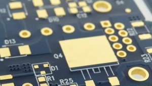
A Gold Plated PCB Board is a printed circuit board that has undergone a specialized surface finishing process in which a thin layer of gold is applied to exposed copper pads, traces, or connectors. The purpose of this layer is not only aesthetic—it provides enhanced electrical conductivity, excellent corrosion resistance, and long-term durability under demanding operating conditions.
Gold has long been associated with luxury and high value, but in the field of electronics, its primary appeal lies in its chemical stability and low electrical resistance. Unlike other surface finishes, gold does not oxidize easily, meaning that the conductive paths on a Gold Plated PCB Board remain clean and reliable for extended periods of time, even in harsh industrial or aerospace environments.
From my perspective, the adoption of Gold Plated PCB Board technology represents a balance between performance and cost. While gold is undeniably more expensive than other finishing materials such as tin, nickel, or even silver, its long-term reliability often offsets the higher initial investment. In mission-critical applications—such as life-supporting medical devices or satellites—failure is not an option, and therefore the durability of gold-plated connections becomes invaluable.
Gold Plated PCB Board
The Historical Development of Gold Plated PCB Board
The idea of plating PCBs with precious metals emerged in the mid-20th century as electronics began to play crucial roles in military communications and aerospace missions. Engineers realized that conventional finishes degraded too quickly in high-humidity, high-vibration, or high-temperature environments. Gold, with its unique combination of electrical and chemical stability, became the obvious solution.
In the early days, full-board gold plating was common, but this was economically unsustainable. Over time, techniques such as electroless nickel immersion gold (ENIG) and hard gold plating were developed to optimize material usage while still delivering the benefits of gold. These innovations paved the way for today’s cost-effective yet reliable Gold Plated PCB Board designs, which are widely adopted across industries.
Materials and Chemistry Behind Gold Plated PCB Board
A Gold Plated PCB Board is not only about adding a shiny finish; it is the outcome of carefully engineered material science. The board itself begins as a substrate such as FR-4 fiberglass, polyimide for flexible circuits, or advanced laminates for high-frequency designs. What distinguishes the Gold Plated PCB Board is the thin plating layer of gold, which typically rests on a nickel barrier.
The nickel layer is critical—it prevents copper from migrating into the gold, which could otherwise weaken solder joints and reduce conductivity. On top of this barrier, gold is deposited, often through processes such as electroless plating, immersion plating, or electroplating. Each method provides distinct benefits:
-
Electroless nickel immersion gold (ENIG): Widely used due to flat surface quality, ideal for fine-pitch components.
-
Hard gold plating: Offers durability against repeated mechanical wear, perfect for connectors and edge contacts.
-
Immersion gold plating: Provides corrosion resistance and excellent solderability, though less mechanically robust.
From a chemical standpoint, gold’s inertness is its main strength. Unlike copper or silver, gold does not oxidize when exposed to air or moisture, making it a near-perfect conductor for sensitive electronic signals. For this reason, Gold Plated PCB Board designs are especially common in RF circuits, aerospace electronics, and mission-critical defense systems.
Manufacturing Process of Gold Plated PCB Board
The manufacturing process of a Gold Plated PCB Board follows the general sequence of PCB fabrication but includes additional plating steps:
-
Substrate preparation – Cleaning and conditioning the base PCB to ensure adhesion of plating layers.
-
Copper patterning – Etching circuits onto the copper layer through photolithography and etching.
-
Nickel barrier deposition – Applying a nickel layer as a diffusion barrier between copper and gold.
-
Gold plating – Depositing gold onto exposed copper pads or connectors using immersion or electroplating.
-
Solder mask application – Protecting non-conductive areas from oxidation and physical damage.
-
Surface inspection and testing – Verifying plating thickness, adhesion, and conductivity to meet quality standards.
This process must be carefully monitored. Too thin a gold layer could compromise corrosion resistance, while too thick a layer significantly increases cost without proportionate benefits. Therefore, balancing gold thickness and application method is one of the central engineering challenges in Gold Plated PCB Board manufacturing.
Surface Finishing Techniques in Gold Plated PCB Board
Surface finishing is one of the most critical aspects of Gold Plated PCB Board design because it directly influences solderability, corrosion resistance, and long-term reliability. There are several finishing techniques:
-
ENIG (Electroless Nickel Immersion Gold): Currently the most popular finish, offering flat surfaces ideal for modern SMT (surface mount technology). It provides excellent solder joint reliability and is used in high-density interconnect boards.
-
Hard Gold Plating: Used mainly for edge connectors, SIM card slots, and keyboard contacts where durability against repeated mating cycles is essential.
-
Immersion Gold Alone: Applied for specialized applications, though less common due to its weaker mechanical strength compared to ENIG or hard gold.
One of the subtle challenges in finishing is “black pad syndrome”, which occurs when the nickel surface beneath the gold develops non-uniformities. This issue highlights why process control and manufacturer expertise are vital. A Gold Plated PCB Board produced without proper quality management could suffer from weak solder joints, leading to premature system failure.
Advantages of Gold Plated PCB Board in Modern Electronics
The advantages of a Gold Plated PCB Board extend across electrical, mechanical, and environmental dimensions. Some of the key benefits include:
-
Superior Conductivity – Gold offers consistent low-resistance connections, essential for high-frequency and high-speed circuits.
-
Corrosion Resistance – Unlike silver or copper, gold does not tarnish, ensuring long-term stability.
-
Durability in Harsh Environments – High humidity, temperature fluctuations, and chemical exposure are less damaging to gold finishes.
-
Excellent Solderability – Smooth surfaces enhance solder joint quality, reducing the risk of cold joints or bridging.
-
Wear Resistance (for hard gold) – Gold’s hardness provides resilience in connectors that undergo repeated mechanical contact.
From my perspective, the key value of Gold Plated PCB Board technology is its predictability. Engineers can design knowing that contact resistance will remain stable over time, even in mission-critical systems. This reduces the need for overdesign and increases overall system efficiency.
Reliability and Durability of Gold Plated PCB Board
One of the strongest reasons engineers choose a Gold Plated PCB Board is its superior reliability in demanding conditions. Unlike other surface finishes such as HASL (Hot Air Solder Leveling) or OSP (Organic Solderability Preservative), gold offers consistent performance across long product lifetimes.
Key aspects of reliability include:
-
Stable Contact Resistance: Because gold does not oxidize or tarnish, the resistance at connector interfaces remains consistent, even after years of use.
-
Long Shelf Life: Gold-plated surfaces maintain solderability far longer than untreated copper or tin finishes.
-
Resistance to Harsh Environments: High humidity, vibration, salt spray, and temperature fluctuations affect gold less than other metals.
From my perspective, the reliability of a Gold Plated PCB Board is not merely about its surface but also about how it simplifies system-level reliability engineering. When component contacts and interconnects are predictable, engineers can design with tighter tolerances, reducing unnecessary redundancies. This is crucial for aerospace or defense projects where weight, space, and cost constraints are strict.
Electrical Performance Benefits of Gold Plated PCB Board
A Gold Plated PCB Board is not just about surviving harsh environments—it also improves electrical performance. For high-frequency, high-speed, and precision analog circuits, surface finish can influence signal integrity significantly.
Electrical benefits include:
-
Low Contact Resistance: Ensures efficient current flow, critical for RF applications and fast-switching logic circuits.
-
Consistent Impedance: A flat, uniform gold surface supports predictable transmission line behavior, improving signal quality.
-
Reduced Noise and Crosstalk: Cleaner, more stable interconnections help minimize electromagnetic interference (EMI).
-
High-Frequency Stability: At microwave frequencies, even minor oxidation layers can degrade performance. Gold avoids this issue entirely.
From my engineering perspective, this is where a Gold Plated PCB Board justifies its cost. In consumer electronics, such refinements might be unnecessary. But in radar systems, 5G base stations, and medical imaging equipment, where nanoseconds and millivolts matter, the benefits are undeniable.
Comparing Gold Plated PCB Board with Other Surface Finishes
When selecting a finishing method for PCBs, engineers often compare a Gold Plated PCB Board against other common finishes such as HASL, OSP, tin, or silver. Each has advantages depending on cost, reliability, and application requirements.
Key Comparisons:
-
HASL (Hot Air Solder Leveling):
-
Pros: Low cost, easy soldering.
-
Cons: Uneven surface, not suitable for fine-pitch components.
-
Verdict: Adequate for consumer electronics, but not competitive with Gold Plated PCB Board in high-density or mission-critical designs.
-
-
OSP (Organic Solderability Preservative):
-
Pros: Very low cost, environmentally friendly.
-
Cons: Short shelf life, poor durability in harsh environments.
-
Verdict: Suitable for short-life consumer products, but unreliable compared to Gold Plated PCB Board.
-
-
Immersion Tin and Silver:
-
Pros: Better conductivity than HASL, smoother surfaces.
-
Cons: Susceptible to oxidation and tarnishing.
-
Verdict: Useful in mid-range electronics, but inferior to gold’s longevity and stability.
-
-
Gold Plating:
-
Pros: Excellent conductivity, corrosion resistance, mechanical durability.
-
Cons: Higher cost due to gold’s price.
-
Verdict: Justified in aerospace, military, telecom, and medical sectors where reliability outweighs cost.
-
From my perspective, while cost-sensitive industries will often default to OSP or HASL, long-term performance almost always tips the balance in favor of Gold Plated PCB Board for high-reliability sectors.
Conclusion: The Role of Gold Plated PCB Board in Next-Generation Electronics
The Gold Plated PCB Board remains one of the most important technologies in the field of electronics. While cost considerations limit its use in consumer-grade products, its unmatched reliability, conductivity, and environmental resistance make it indispensable for aerospace, defense, telecom, and medical sectors.
From my perspective, the adoption of gold plating represents a philosophy of engineering—choosing reliability and predictability over short-term cost savings. As electronics push further into hostile environments and life-critical roles, the Gold Plated PCB Board will continue to be a trusted foundation.
FAQs About Gold Plated PCB Board
1. What is the difference between rolled copper foil and electrolytic copper foil?
Rolled copper foil is produced by mechanically rolling copper into thin sheets, offering better surface quality and mechanical strength. Electrolytic copper foil is deposited via an electrolytic process and is more flexible and cost-effective.
2. Why is nickel used under gold in a Gold Plated PCB Board?
Nickel acts as a diffusion barrier to prevent copper migration into the gold layer. Without it, the gold surface could degrade, leading to weak solder joints.
3. How thick should the gold layer be in a Gold Plated PCB Board?
Thickness varies depending on application. For connectors, hard gold plating may require 30–50 microinches. For ENIG, immersion gold layers are typically 2–5 microinches.
4. Is a Gold Plated PCB Board suitable for consumer electronics?
Not usually, because gold adds cost. It is typically reserved for aerospace, medical, and military applications where reliability is critical. However, high-end smartphones and luxury devices sometimes use gold finishes.
5. How does SQ PCB ensure quality in Gold Plated PCB Board production?
SQ PCB uses automated plating systems, tight process controls, and international certification standards. This ensures consistent thickness, adhesion, and durability, making their products reliable for demanding applications.

- long board pcb
- Flexible PCBs
- Special PCB
- Express Printed Circuit Board
- Pcb Prototype
- LED PCB
- PCB
- Printed Circuit Board
- Pcb meaning
- Pcb manufacturer
- Rigid pcb board
- Rigid Flex PCB
 Quote
Quote
 E-mail