Gold Flash vs Gold Plating: Understanding the Differences and Applications
When it comes to enhancing the durability and performance of electronic components, gold plating and gold flash are two commonly used methods for surface finishing. Both processes provide excellent corrosion resistance, improve electrical conductivity, and offer aesthetic appeal. However, they differ significantly in terms of thickness, application, and cost. This article will explore the differences between gold flash and gold plating, their respective advantages, and the best applications for each.
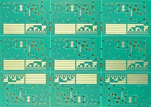
Gold Flash vs Gold Plating
What is Gold Flash?
Gold flash, also known as “gold flash plating,” is a thin coating of gold applied to a substrate, typically using an electroplating process. This process involves depositing a very thin layer of gold, often less than 0.1 microns, over the surface of the base material. The gold flash is often used as a base layer before further metal finishing or as a protective coating for connectors and contacts in electronic devices.
Key Characteristics of Gold Flash
-
Thin Layer
Gold flash is characterized by its ultra-thin gold layer. This makes it more cost-effective compared to thicker gold plating. The layer of gold flash is typically measured in microns or even nanometers. -
Cost-Effective
Due to the thinness of the gold layer, gold flash is less expensive than traditional gold plating. It is a preferred option when cost is a significant factor, and only a thin gold coating is needed for performance. -
Improved Conductivity and Protection
Despite its thinness, gold flash provides improved electrical conductivity and a protective layer against oxidation, making it useful in applications that require moderate corrosion resistance and conductivity.
Common Uses of Gold Flash
- Connector Pins: Gold flash is commonly used in the plating of connector pins where a thin protective coating is sufficient to ensure reliable electrical conductivity and prevent corrosion.
- Printed Circuit Boards (PCBs): In some cases, gold flash is used for specific parts of PCBs, where only a light coating is required to ensure a smooth surface for soldering.
- Cosmetic Finishing: Gold flash is sometimes used for aesthetic purposes in consumer electronics and jewelry, where a shiny, gold-like appearance is needed without significant cost.
What is Gold Plating?
Gold plating, on the other hand, involves the application of a thicker layer of gold over a substrate, typically through an electroplating process. The thickness of gold plating varies, but it is typically much thicker than gold flash, ranging from 0.1 microns to several microns. Gold plating provides a more substantial layer of gold that offers greater durability, corrosion resistance, and enhanced electrical performance.
Key Characteristics of Gold Plating
-
Thicker Layer
Gold plating features a thicker layer of gold, making it more durable and long-lasting compared to gold flash. The plating is often several microns thick, providing superior protection against corrosion and wear. -
Enhanced Durability
Gold plating provides enhanced durability, which makes it ideal for applications requiring long-term reliability and protection. It can endure higher mechanical stresses and is less prone to wear over time compared to gold flash. -
Better Electrical Performance
Due to the thicker gold layer, gold-plated surfaces offer superior electrical conductivity. This makes gold plating an ideal choice for applications where reliable and consistent electrical performance is crucial.
Common Uses of Gold Plating
- High-End Connectors: Gold plating is commonly used in high-performance connectors and electronic components where reliability and durability are paramount.
- PCB Components: Gold plating is often used on high-quality PCBs, particularly in applications such as aerospace, military, and medical devices, where performance and longevity are critical.
- Memories and Storage Devices: Gold-plated contacts are often used in memory modules, hard drives, and other storage devices for reliable data transmission and connection.
Gold Flash vs Gold Plating: Key Differences
While both gold flash and gold plating provide similar benefits in terms of corrosion resistance and electrical performance, they differ in several key areas:
1. Thickness
One of the most significant differences between gold flash and gold plating is the thickness of the gold layer. Gold flash typically features a very thin layer of gold, often less than 0.1 microns, while gold plating has a thicker layer, typically ranging from 0.1 microns to several microns thick. The thicker layer in gold plating makes it more durable and resistant to wear and tear.
2. Cost
Due to the thinness of the gold layer, gold flash is generally less expensive than gold plating. Gold flash is a more cost-effective option when a thin gold layer is sufficient for the application. Gold plating, on the other hand, requires more gold and more time to apply, making it a more expensive option.
3. Durability and Wear Resistance
Gold plating is more durable and resistant to mechanical wear compared to gold flash. The thicker layer of gold in gold plating makes it better suited for applications that require long-term performance and resistance to physical stress. Gold flash, with its thin coating, is more susceptible to wear over time.
4. Electrical Performance
While both gold flash and gold plating offer excellent electrical conductivity, gold plating provides superior performance due to the thicker layer of gold. This makes gold plating a better choice for high-performance applications where reliable electrical connection and performance are critical.
5. Applications
Gold flash is typically used in applications where a thin, cost-effective gold coating is sufficient, such as in lower-cost connectors or decorative items. Gold plating, on the other hand, is used in more demanding applications such as high-end connectors, PCBs, and military or aerospace components, where durability, longevity, and performance are essential.
Which One Should You Choose: Gold Flash or Gold Plating?
The decision to use gold flash or gold plating depends on the specific requirements of the application. If you need a thin, cost-effective solution for corrosion resistance or improved electrical conductivity, gold flash may be the right choice. It is suitable for applications where the performance requirements are moderate, and cost is a significant concern.
On the other hand, if durability, long-term performance, and superior electrical conductivity are essential, gold plating is the better option. It is ideal for high-end connectors, military-grade electronics, and other critical applications where reliability and longevity are key.
Conclusion
Gold flash and gold plating are both valuable processes for enhancing the performance of electronic components. Gold flash provides a cost-effective solution with a thin gold coating, ideal for less demanding applications, while gold plating offers superior durability, performance, and reliability with a thicker gold layer. By understanding the key differences and applications of these two processes, you can make an informed decision based on the specific needs of your project, ensuring optimal performance and longevity of your electronic components.

- long board pcb
- Flexible PCBs
- Special PCB
- Express Printed Circuit Board
- Pcb Prototype
- LED PCB
- PCB
- Printed Circuit Board
- Pcb meaning
- Pcb manufacturer
- Rigid pcb board
- Rigid Flex PCB
 Quote
Quote
 E-mail