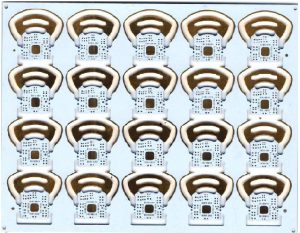
PCB edge plating, also known as plated edges or edge connectors, is an advanced manufacturing technique that enhances the functionality and durability of printed circuit boards (PCBs). By applying a conductive material along the edges of a PCB, this method not only improves electrical connectivity but also ensures better mechanical strength. In a world where PCBs are integral to electronics, edge plating has emerged as a game-changer in PCB manufacturing.
pcb edge plating
2. The Basics of PCB Edge Plating
Definition and Purpose of Edge Plating
Edge plating involves coating the edges of a printed circuit board with a conductive material, such as copper, nickel, or gold. This process creates a robust electrical and mechanical connection between different layers and components, contributing to PCB reliability and durability.
Key Components Involved in Edge Plating
Conductive material, plating equipment, and surface preparation materials are the essential components of edge plating. Copper plating is commonly used as the base material, often layered with nickel plating or gold plating for additional properties like corrosion resistance and enhanced thermal management.
3. Why PCB Edge Plating is Crucial in Modern Electronics
Enhanced Durability for High-Stress Applications
Edge plating reinforces the structural integrity of PCBs, making them suitable for rugged environments such as aerospace and military applications, where PCB wear resistance is critical.
Improved Conductivity and Electrical Performance
By reducing resistance along edges, edge plating ensures seamless electrical connectivity between components, an essential feature for high-power electronics and high-density interconnect PCB designs.
Better Heat Dissipation and Thermal Management
Edge plating aids in dispersing heat, crucial for thermal management in high-power or high-density designs, contributing to overall PCB heat dissipation.
4. Common Applications
PCB edge plating is widely used in various industries, including aerospace and defense for high-reliability communications, industrial equipment for high-power machinery, and consumer electronics for devices such as smartphones and wearables. The benefits extend to multi-layer PCB designs where plating uniformity ensures robust connections.
5. Materials Used
Common Metals
Copper plating, gold plating, and nickel plating are the primary materials used in edge plating. Copper offers excellent conductivity, gold provides superior corrosion resistance, and nickel acts as a barrier layer to prevent diffusion, ensuring long-term PCB structural integrity.
How Material Choices Affect Performance and Cost
The choice of PCB plating materials significantly impacts performance. For instance, gold-plated edges are ideal for premium applications due to their anti-corrosive properties, albeit at a higher cost. Nickel plating is often used for PCB reinforcement, adding durability for high-stress applications.
6. The Process
Preparing the PCB Surface
Cleaning the surface to remove impurities and applying a mask to define the plating area are essential preparation steps for ensuring PCB surface finishing and plating uniformity.
Plating Techniques
Electroplating uses electrical current to deposit metal layers, while electroless plating is a chemical process that ensures uniform deposition without electricity. Both techniques are essential in modern PCB manufacturing.
Ensuring Uniformity and Quality
Precise equipment and regular inspection are critical to achieving uniform plating thickness, an important aspect of PCB reliability and meeting PCB industry standards.
7. Advanced Techniques
Controlled Depth Drilling
This technique ensures precision in plating depth, critical for high-density interconnect PCB applications.
Plating for Multi-Layer and High-Density Interconnect PCBs
Edge plating is especially advantageous for complex multi-layer PCB designs, ensuring reliable interconnections and durability.
Innovations in Edge Plating Technology
Recent advancements include automated plating and AI-driven quality checks, which contribute to environmentally friendly PCB processes and reduced costs.
8. Challenges
Manufacturing challenges include achieving plating uniformity, managing high production costs, and reducing material waste. Solutions include advanced plating techniques, process optimization, and eco-friendly manufacturing practices.
9. Benefits in PCB Design
Enhanced Aesthetic Appeal
Edge plating gives PCBs a professional and polished look, vital for consumer-facing products and advanced PCB technology.
Improved Reliability and Longevity
Plated edges resist wear and environmental factors, extending the PCB’s lifespan and improving PCB corrosion resistance.
Compatibility with Advanced Soldering Processes
Edge plating facilitates secure connections during assembly, even in complex designs, enhancing overall PCB reliability.
10. Key Considerations When Designing for Edge Plating
PCB design tips include ensuring adequate spacing between plated edges and components, using a consistent plating thickness for uniform performance, and selecting PCB plating materials compatible with the edge plating process.
11. Quality Assurance
Inspection Techniques
Optical analysis detects surface irregularities, while X-ray analysis ensures internal consistency and layer alignment. Regular inspections are vital for adhering to ISO certifications and UL certifications, ensuring high-quality PCB manufacturing.
Standards and Certifications
Adhering to PCB industry standards ensures consistent quality and reliability in edge plating.
12. Comparing PCB Edge Plating with Other Plating Techniques
Edge plating enhances durability and aesthetics compared to other methods like hard gold plating or through-hole plating, which are better suited for specific designs but may lack versatility for multi-layer PCB applications.
13. Environmental and Sustainability Aspects of Edge Plating
Eco-Friendly Plating Practices
Using non-toxic chemicals and recycling materials helps minimize environmental impact. Automated plating also contributes to more sustainable manufacturing.
Reducing Waste and Energy Consumption
Automation and process optimization significantly cut down energy usage and material waste, making edge plating an eco-friendly manufacturing process.
14. Trends and Future Developments
Automation in Plating Processes
AI and robotics are revolutionizing edge plating, ensuring precision, scalability, and alignment with PCB trends.
Emerging Materials and Techniques
Innovations include environmentally friendly plating materials and hybrid techniques for enhanced performance in high-power electronics and high-stress applications.
15. Conclusion
PCB edge plating is a transformative technology in the world of electronics manufacturing. From enhancing durability and PCB structural integrity to improving thermal management and electrical connectivity, it’s a crucial aspect of modern PCB design. As technologies evolve, edge plating will continue to play a vital role in enabling high-performance, reliable electronics while aligning with PCB industry standards.
Also can check it on linkedin
our linken sqpcb.com
https://www.linkedin.com/feed/update/urn:li:activity:
7097167729337532416

- long board pcb
- Flexible PCBs
- Special PCB
- Express Printed Circuit Board
- Pcb Prototype
- LED PCB
- PCB
- Printed Circuit Board
- Pcb meaning
- Pcb manufacturer
- Rigid pcb board
- Rigid Flex PCB
 Quote
Quote
 E-mail