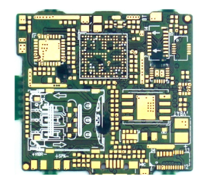
Exploring Multilayer PCBs, Printed circuit boards (PCBs) form the foundation of modern electronic devices. Among them, multilayer PCBs stand out for their complexity, efficiency, and versatility. With their ability to support high-performance applications, multilayer PCBs have become a vital component in various industries. This guide explores the essential aspects of multilayer PCBs, including their structure, benefits, design considerations, manufacturing process, and applications.

Exploring Multilayer PCBs
What is a Multilayer PCB?
A multilayer PCB consists of multiple conductive layers of copper foil separated by insulating material, all laminated into a single board. Unlike single-layer or double-layer PCBs, multilayer PCBs incorporate three or more layers, often exceeding a dozen in high-performance applications. These additional layers allow for more advanced circuit designs, better electrical performance, and improved space utilization, making them essential for complex electronic devices.
Structure and Design of Exploring Multilayer PCBs
Multilayer PCBs have a sophisticated structure that enhances their functionality:
- Core Layer: A rigid base substrate that provides structural integrity and stability.
- Inner Layers: Multiple layers of copper circuits embedded within the PCB, allowing for compact and efficient circuit routing.
- Prepreg: Insulating material placed between layers to enhance adhesion, electrical insulation, and mechanical strength.
- Outer Layers: The top and bottom conductive layers where most components are placed and connected.
- Vias: Conductive pathways that interconnect different layers for complex circuit designs, including through-hole, blind, and buried vias.
The design of multilayer PCBs requires advanced techniques and tools, such as Computer-Aided Design (CAD) software, to optimize signal routing, ensure minimal signal loss, and reduce interference. Factors such as signal integrity, impedance control, thermal management, and layer stack-up must be carefully considered during the design phase.
Manufacturing Process of Exploring Multilayer PCBs
The production of multilayer PCBs involves several intricate steps to ensure quality and reliability:
- Design & Layout: Engineers create detailed schematics and layouts using specialized CAD software to define circuit paths, component placement, and layer arrangements.
- Material Preparation: The selection of high-quality substrates, copper foils, and insulating materials is critical to achieving desired performance characteristics.
- Inner Layer Processing: Copper layers are laminated onto core materials, etched to form circuit patterns, and subjected to oxidation prevention treatments.
- Layer Alignment & Lamination: Multiple layers are precisely aligned and bonded together through high-temperature and high-pressure lamination processes.
- Drilling & Plating: Holes are drilled for vias and component mounting, followed by copper plating to establish electrical connections.
- Etching & Imaging: The circuit patterns are further refined using chemical etching and photolithography techniques.
- Surface Finishing: Protective finishes such as HASL, ENIG, or OSP are applied to enhance solderability and corrosion resistance.
- Testing & Quality Control: Each board undergoes rigorous testing, including electrical testing, X-ray inspection, and automated optical inspection (AOI), to ensure defect-free performance.
Advantages of Exploring Multilayer PCBs
Multilayer PCBs offer several advantages over their single-layer and double-layer counterparts:
- Higher Component Density: Allows more components to fit within a compact design, making them ideal for modern, high-performance electronic devices.
- Improved Electrical Performance: Supports complex circuitry with enhanced signal integrity, reduced signal loss, and better power distribution.
- Minimized Electromagnetic Interference (EMI): Layer stacking and strategic design help reduce EMI and crosstalk between signals, ensuring reliable operation.
- Increased Durability: The lamination process enhances mechanical strength, making multilayer PCBs resistant to environmental stress and prolonged usage.
- Greater Design Flexibility: Provides engineers with more options for designing intricate circuits with precise control over electrical characteristics.
- Better Heat Dissipation: The multilayer structure helps in efficient heat dissipation, reducing the risk of component overheating and failure.
Applications of Exploring Multilayer PCBs
Due to their efficiency and reliability, multilayer PCBs are used across various industries:
- Consumer Electronics: Found in smartphones, laptops, tablets, and wearable devices to enable compact, high-performance products.
- Medical Devices: Essential for MRI machines, pacemakers, medical imaging systems, and other advanced diagnostic equipment requiring precision and reliability.
- Automotive Electronics: Used in vehicle navigation systems, safety components, ADAS (Advanced Driver Assistance Systems), and infotainment systems.
- Aerospace and Defense: High-performance multilayer PCBs withstand extreme conditions in aircraft, satellites, radar systems, and military-grade equipment.
- Telecommunications: Support high-speed data transmission, 5G networks, and networking infrastructure essential for global connectivity.
- Industrial Automation: Used in robotic systems, industrial control units, and automation equipment for enhanced efficiency and reliability.
Choosing the Right PCB Manufacturer
Selecting a reliable PCB manufacturer is critical for achieving optimal performance. A leading manufacturer should offer:
- Advanced Technology: Utilization of cutting-edge manufacturing processes, including HDI (High-Density Interconnect) and flexible PCB technology, for precision and reliability.
- Customization Options: Ability to create tailored solutions to meet specific industry requirements, including custom layer stack-ups and material choices.
- Quality Assurance: Rigorous testing and quality control procedures, such as AOI, flying probe testing, and thermal cycling tests, to ensure compliance with industry standards.
- Global Supply Chain: Efficient production and timely delivery, ensuring customers receive high-quality PCBs without delays.
- Competitive Pricing: Cost-effective solutions without compromising quality, helping businesses optimize their electronics manufacturing processes.
Conclusion
Exploring Multilayer PCBs play a crucial role in the advancement of modern electronics. Their superior design, enhanced performance, and wide-ranging applications make them indispensable across industries. As technology continues to evolve, the demand for high-quality multilayer PCBs will only grow, driving innovation in various sectors. Businesses seeking robust and efficient PCB solutions should partner with experienced manufacturers to ensure reliability, precision, and long-term performance in their electronic products.
our linkedin sqpcb.com
- long board pcb
- Flexible PCBs
- Special PCB
- Express Printed Circuit Board
- Pcb Prototype
- LED PCB
- PCB
- Printed Circuit Board
- Pcb meaning
- Pcb manufacturer
- Rigid pcb board
- Rigid Flex PCB

 Quote
Quote
 E-mail