What is a Multilayer PCB?
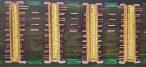
A multilayer PCB consists of multiple conductive layers, typically copper, separated by insulating layers. These layers are laminated together under high heat and pressure, resulting in a single board. This design allows engineers to increase the complexity of the circuits while reducing the overall size of the PCB. The ability to integrate more layers in a single PCB is crucial for devices that require compactness and performance.
Key Features of Multilayer PCBs:
- Multiple Conductive Layers: These boards have more than two layers of copper that are interconnected, providing greater functionality and supporting complex circuit designs.
- Compact Design: The additional layers allow for high-density circuits, making multilayer PCBs ideal for devices that require compactness.
- High Performance: The more layers a PCB has, the better it can handle complex electrical signals and power distribution, making it suitable for high-speed applications.
Manufacturing Process of Multilayer PCBs
The manufacturing of multilayer PCBs is a precise and intricate process that requires careful attention to detail. The process involves several critical steps to ensure the integrity, performance, and reliability of the final product:
1. Design and Layout
The process starts with the design phase, where engineers create the layout for the PCB using Computer-Aided Design (CAD) software. This step includes designing the routing of copper traces, component placement, and determining the number of layers required. The design is then converted into Gerber files for manufacturing.
2. Material Preparation
The next step involves preparing the base material, typically made from fiberglass (FR4), which serves as the primary substrate for the PCB. Copper foil is then applied to each side of the substrate. The number of copper layers will depend on the design requirements.
3. Inner Layer Imaging
After the copper is applied, the inner layers of the PCB are printed with the circuit design using photoresist material. The photolithography process is used to transfer the design onto the copper layers, ensuring that the copper traces are correctly positioned.
4. Etching
Once the design is transferred, the next step is etching, which involves using a chemical solution to remove the exposed copper from the areas not protected by the photoresist. This leaves the desired copper traces that will form the conductive pathways.
5. Lamination
The etched inner layers are then laminated together with insulating layers (often made from epoxy resin) in between. The layers are bonded together using heat and pressure to ensure that no air gaps are present and that the layers are firmly adhered to each other.
6. Drilling
After lamination, precise holes are drilled into the PCB. These holes are called vias, and they provide electrical connections between the different layers of the PCB. Vias allow signals and power to flow from one layer to another, enabling complex designs. Once drilled, the vias are plated with copper to ensure electrical continuity.
7. Outer Layer Imaging and Etching
The outer layers of the PCB are imaged and etched in a similar manner to the inner layers. This step defines the circuit paths on the outer surfaces, which will later be used for the connection of external components.
8. Solder Mask Application
Once the etching is complete, a solder mask is applied to the surface of the PCB. This mask protects the copper traces from oxidation and prevents solder bridges during component assembly. The mask leaves exposed areas where components will be soldered.
9. Surface Finish
The exposed copper pads are treated with a surface finish, such as HASL (Hot Air Solder Leveling), ENIG (Electroless Nickel Immersion Gold), or OSP (Organic Solderability Preservatives). These finishes enhance the solderability and protect the copper from oxidation.
10. Testing and Inspection
The final PCB undergoes various tests, including electrical testing to ensure the connections are intact and functional. Automated Optical Inspection (AOI) is used to visually inspect the board for any defects, such as misalignment or flaws in the etching process.
Applications of Multilayer PCBs
Multilayer PCBs are used in a variety of industries where space efficiency, performance, and reliability are paramount. Below are some key applications:
1. Consumer Electronics
Multilayer PCBs are essential in smartphones, tablets, laptops, and wearable technology. The complexity of these devices requires compact and high-performance PCBs to support various components such as processors, memory, and sensors.
2. Telecommunications
Telecommunication equipment, including routers, switches, and base stations, relies on multilayer PCBs for high-speed data transmission and signal integrity. The ability to route signals through multiple layers helps ensure reliable connectivity and performance in data-heavy environments.
3. Medical Devices
In the medical industry, multilayer PCBs are used in diagnostic equipment, MRI machines, CT scanners, and portable monitoring devices. These PCBs must meet strict performance standards and operate reliably in demanding environments.
4. Automotive
Modern vehicles incorporate advanced electronic systems, such as advanced driver-assistance systems (ADAS), navigation systems, and infotainment systems, all of which use multilayer PCBs. These boards ensure the reliability and performance required in automotive applications, even under challenging conditions.
5. Aerospace and Defense
In aerospace and defense, multilayer PCBs are crucial for systems like avionics, radar, and communication equipment. These systems require high-performance, high-reliability PCBs to function in extreme environments.
6. Industrial Automation
Multilayer PCBs are widely used in industrial automation systems, including control systems, sensors, and robotics. These systems depend on high-performance PCBs to ensure the efficient and reliable operation of machinery.
Conclusion
Multilayer PCBs are a cornerstone of modern electronics, enabling the development of compact, high-performance, and complex circuits. The manufacturing process, though intricate, ensures the precision and reliability needed for advanced applications in various industries, including telecommunications, medical devices, automotive, aerospace, and industrial automation. As technology continues to evolve, the demand for multilayer PCBs will only increase, driving innovation and supporting the development of more sophisticated and reliable electronic devices.

 Quote
Quote
 E-mail