1. Introduction
In modern electronics manufacturing, printed circuit boards (PCBs) serve as the central nervous system of virtually every device—from consumer gadgets to critical aerospace systems. As device complexity increases and the demand for smaller, faster, and more reliable electronics rises, PCB technologies must evolve in tandem. One such innovation that has played a quiet yet vital role in maintaining signal integrity, enhancing component isolation, and improving production yields is the application of solder mask dams (often abbreviated as DAMS).
Though they might seem trivial compared to more conspicuous features like vias, traces, or multilayer architectures, solder mask dams are micro-scale barriers intentionally designed into the PCB layout to prevent solder migration during the reflow or wave soldering process. Their strategic placement has a significant impact on the performance, durability, and functionality of a final product. Particularly in densely populated boards, solder mask dams are crucial for maintaining circuit integrity.
The purpose of this article is to explore in depth the advantages and applications of solder mask DAMS in PCB manufacturing—covering their chemical composition, design strategies, roles in various technologies like HDI and rigid-flex, and how they enable advances in miniaturization and thermal management. In addition to technical insights, I will include my own observations on how solder mask DAMS contribute to the overall sustainability and efficiency of the electronics supply chain.
While the use of solder mask dams is widespread in the PCB industry, detailed technical discussions are often missing in mainstream PCB education. As such, this article aims to bridge that gap for engineers, designers, and even procurement specialists who want to understand the hidden structures that often determine the success of PCB assemblies.
Solder mask dams do not operate in isolation; they interact with other PCB features and processes. From impedance control to prevention of bridging and signal interference, their impact is far-reaching. But perhaps more importantly, they embody the principle that in PCB design, microscopic features can yield macroscopic advantages.
As we navigate the intricacies of this article, we will highlight not only where solder mask dams are used but also why they are essential in high-reliability applications. Furthermore, I will offer a forward-looking perspective on how this technique might evolve with trends such as AI-driven PCB design, additive manufacturing, and green electronics.
Understanding the significance of solder mask DAMS is not merely an academic exercise. It is a strategic imperative for engineers and manufacturers committed to delivering quality and innovation in an ever-competitive global electronics market.
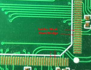
Solder Mask DAMS
2. Fundamentals of Solder Mask DAMS in PCB Design
In the vast world of PCB manufacturing, design elements often vary in scale, from large multilayer stack-ups to microscopic layout tweaks. Among these seemingly minor yet functionally critical features are solder mask DAMS—narrow bands of solder mask material placed between closely spaced surface mount pads to contain solder flow and prevent bridging. Despite their simplicity, understanding their fundamentals is essential for ensuring both functional reliability and manufacturability of high-performance circuit boards.
2.1 The Purpose of Solder Mask DAMS in PCB Design
The primary role of solder mask DAMS in PCB design is to act as physical barriers that isolate adjacent solder pads, particularly in densely packed areas of the board. These dams prevent unintended electrical connections caused by solder migration during reflow or wave soldering. This is especially critical in fine-pitch components such as QFNs, BGAs, and CSPs, where spacing between leads can be less than 0.5 mm.
Without solder mask dams, surface tension during soldering can cause solder to bridge adjacent pads, leading to short circuits, signal interference, or total functional failure. Therefore, even though these dams may measure only 0.1–0.2 mm in width, they perform a disproportionately important role in the successful assembly of electronic systems.
2.2 Physical and Geometrical Characteristics of Solder Mask DAMS
Solder mask DAMS are defined by their width, height, and placement. The typical dimensions are:
-
Width: ≥ 0.1 mm (100 µm), depending on PCB fabrication capabilities
-
Height: Equal to the solder mask thickness, typically ranging from 10–50 µm
-
Spacing: Positioned between pads of surface mount components
Designers must consider the minimum solder mask dam width allowed by the manufacturer, which varies by fabrication house. Too thin a dam, and the mask may not properly adhere; too wide, and the dam may encroach on the pad area, reducing solderability.
An often-overlooked constraint is registration accuracy. Misalignment between the solder mask and copper layers during fabrication can compromise the integrity of the dam. Designers typically include tolerances or utilize design rules from their board house to minimize such risks.
2.3 Key Parameters in Solder Mask DAMS Design
Three core factors dictate the success of solder mask DAMS in PCB layout:
-
Pad Pitch: The closer the pads, the narrower the possible solder mask dams. Fine-pitch components may not accommodate any dam at all.
-
Solder Mask Type: Liquid Photo-Imageable (LPI) masks offer better definition than older epoxy-based masks and are more suitable for precision DAMS.
-
PCB Layer Stack-Up: For multilayer PCBs, the top and bottom layers may need different solder mask strategies based on thermal behavior and surface treatment.
To maximize effectiveness, designers may refer to IPC standards (e.g., IPC-SM-840) and manufacturer-specific design guides. CAD tools like Altium Designer, KiCad, or Mentor Graphics PADS typically include solder mask dam constraints as part of their Design Rule Checks (DRC).
2.4 Design for Manufacturability (DFM) and Solder Mask DAMS
Incorporating solder mask DAMS into a PCB layout is not only a matter of electrical performance but also of Design for Manufacturability (DFM). Well-defined solder mask dams:
-
Enhance process repeatability during automated soldering
-
Reduce touch-up requirements and manual rework
-
Improve first-pass yield, especially for high-volume production
From a DFM perspective, solder mask DAMS serve as an alignment guide for pick-and-place machines, help prevent tombstoning of passive components, and act as visual indicators during inspection.
However, overly aggressive use of dams—such as placing them where they are not needed or making them too thick—can interfere with solder paste deposition and create reliability problems. As with all design elements, balance is key.
2.5 Real-World Examples of Solder Mask DAMS in Use
In practical terms, solder mask DAMS are most commonly found in:
-
Ball Grid Arrays (BGAs) with pad pitches as small as 0.4 mm
-
Memory modules where fine-pitch DRAM or flash components demand high precision
-
Wearables and IoT devices where board area is severely constrained
-
Automotive control units requiring thermal stability and high vibration tolerance
For example, in a smartwatch PCB where space is at a premium and the density of components is extremely high, solder mask dams can be the difference between a functioning device and one that suffers intermittent shorts after minor mechanical stress.
2.6 My Reflections on the Fundamentals of Solder Mask DAMS
What strikes me about solder mask DAMS is how invisible engineering often holds together complex systems. In an era dominated by conversations around AI chips and 5G antennas, it’s easy to overlook the critical impact of micro-scale features. Yet without these dams, many consumer electronics would fail not at the software or system level, but due to simple physical flaws like solder bridging.
I believe the fundamental lesson here is that robust PCB design is not just about innovation—it’s about precision and restraint. Solder mask DAMS exemplify this principle by quietly safeguarding performance in countless devices.
3. Material Composition and Chemical Properties of Solder Mask DAMS
Understanding the material composition and chemical behavior of solder mask DAMS is essential for grasping why these features can withstand thermal, mechanical, and chemical stress during PCB manufacturing and operation. The functionality and reliability of these micro-barriers are directly linked to the specific formulation of the solder mask material and how it behaves throughout the PCB assembly lifecycle.
3.1 Base Materials Used in Solder Mask DAMS
Solder mask DAMS are fabricated using the same base material as the rest of the solder mask layer on the PCB—typically liquid photo-imageable (LPI) solder mask, though dry film variants are also used in niche applications. The LPI formulation comprises several key components:
-
Epoxy resin or acrylic resin base: Provides structural stability and thermal resistance.
-
Photo-initiators: Allow the solder mask to harden selectively when exposed to UV light.
-
Color pigments: Most commonly green, but available in black, blue, red, and white.
-
Fillers: Improve mechanical strength and control viscosity.
-
Solvents: Allow for smooth application and viscosity control before curing.
Among these, epoxy-based LPI solder masks are the most widely adopted due to their excellent adhesion, low cost, and durability. The same properties that make them suitable for general PCB protection also enable solder mask DAMS to perform reliably during soldering and long-term use.
3.2 Curing Mechanisms and Cross-Linking in Solder Mask DAMS
The physical robustness of solder mask DAMS is largely determined during the curing stage of solder mask processing. After applying the solder mask and selectively exposing it to UV light (through photolithography), the exposed regions undergo polymer cross-linking, which transforms the liquid resin into a hard thermoset material.
Key factors influencing this process include:
-
UV wavelength and intensity: Affects the depth and completeness of the cure.
-
Post-bake temperature: Usually around 150–180°C, which finalizes the hardening.
-
Curing duration: Typically 30–60 minutes in convection or IR ovens.
Well-cured solder mask DAMS exhibit excellent dimensional stability, solvent resistance, and thermal endurance, ensuring that they do not melt, blister, or detach during lead-free soldering processes, which can reach temperatures of up to 260°C.
3.3 Chemical Resistance of Solder Mask DAMS
One of the key benefits of solder mask DAMS lies in their ability to withstand harsh chemical environments. During PCB fabrication and cleaning processes, PCBs are exposed to numerous chemicals, including:
-
Fluxes (acidic or mildly corrosive)
-
Solvents (e.g., isopropyl alcohol, acetone)
-
De-fluxing agents
-
Saponifiers (alkaline cleaners)
-
Aqueous or semi-aqueous detergents
Solder mask DAMS, by virtue of their polymeric structure, exhibit strong resistance to acids and alkalis, as well as minimal swelling or softening when exposed to cleaning agents. This property is vital for high-reliability PCBs used in automotive, aerospace, and industrial sectors, where harsh environmental conditions are standard.
3.4 Thermal Properties of Solder Mask DAMS Materials
Temperature-related stresses are among the most common causes of material failure in PCBs. Therefore, solder mask DAMS must be able to maintain their shape, adhesion, and barrier properties throughout multiple thermal cycles.
Key thermal properties of typical solder mask DAMS materials include:
-
Glass Transition Temperature (Tg): 120–150°C
-
Decomposition Temperature (Td): >280°C
-
Thermal Conductivity: Very low, typically <0.3 W/mK
-
CTE (Coefficient of Thermal Expansion): Matched to the PCB substrate to avoid stress-induced cracking
It’s important to note that thermal mismatches between the copper pads, solder mask DAMS, and underlying FR-4 laminate can create micro-fractures if not carefully managed. Therefore, material engineers often tune the epoxy formulation to align its thermal expansion characteristics with those of the copper and substrate layers.
3.5 Adhesion and Surface Interaction of Solder Mask DAMS
For solder mask DAMS to be effective, they must bond securely to the copper surface and resist delamination, especially when exposed to moisture or vibration. The adhesion strength of the dam is influenced by:
-
Surface roughness of the copper (mechanical anchoring)
-
Cleanliness of the surface before solder mask application
-
Presence of oxide layers, which can be mitigated using pre-treatment like micro-etching
-
Solder mask formulation, especially adhesion promoters
Manufacturers may perform cross-cut adhesion tests or thermal shock cycles to validate the mechanical integrity of the solder mask DAMS layer. These tests simulate real-world stress conditions and ensure that the mask won’t peel off or crack in the field.
3.6 Evolution of Solder Mask Materials for DAMS Applications
Recent years have witnessed the emergence of high-resolution solder mask technologies designed to support finer features, including narrower and taller dams. These advanced materials are often:
-
Low-halogen or halogen-free for environmental compliance (RoHS, REACH)
-
Higher Tg for compatibility with lead-free processes
-
Laser-patternable for extreme precision in HDI and IC substrates
Emerging technologies such as inkjet-applied solder masks are being explored as a way to improve the precision and repeatability of solder mask DAMS without the constraints of traditional photolithography.
3.7 My Reflections on the Material Science Behind Solder Mask DAMS
As someone fascinated by the intersection of materials engineering and electronics, I see the chemistry of solder mask DAMS as a triumph of micro-level innovation. It reminds us that a circuit’s performance is not solely governed by its layout or logic—it is also deeply tied to the materials that hold it together.
The ability of solder mask DAMS to survive mechanical stress, high heat, and chemical exposure reflects a deep commitment to quality at every layer of design. It’s not just about keeping solder in place; it’s about ensuring that each electrical path stays clean, consistent, and isolated—no matter what the environment throws at it.
4. Design Strategies Using Solder Mask DAMS in High-Density Boards
The increasing demand for compact, high-performance electronics has led to rapid adoption of high-density interconnect (HDI) PCB designs. These boards, characterized by fine-pitch components, stacked microvias, and minimal real estate, require a level of design precision that leaves no room for error. Among the many techniques that help maintain functionality and yield in HDI layouts, solder mask DAMS play an essential role in enhancing isolation and manufacturability at the micro-scale.
4.1 The Role of Solder Mask DAMS in High-Density Layouts
In high-density layouts, surface mount component pads are packed tightly together, often at pitches of 0.5 mm or less. In such environments, the risk of solder bridging increases exponentially, especially during reflow soldering processes. Here, solder mask DAMS are used as physical barriers that confine solder paste to the intended pads and prevent migration to adjacent lands.
While in traditional layouts, the absence of solder mask DAMS may not cause catastrophic failure, in HDI designs, a single bridged connection could compromise the entire assembly. Therefore, solder mask DAMS are not optional—they are often a necessity.
4.2 Balancing Pad Pitch and Solder Mask DAMS Dimensions
One of the core challenges in HDI design is finding the right balance between pad pitch and the minimum manufacturable dam width. As the pitch decreases, the available space for solder mask DAMS diminishes. Designers must decide whether to:
-
Include narrower solder mask DAMS, potentially challenging fabrication capabilities
-
Remove solder mask between pads (creating a “mask-defined” pad)
-
Use solder mask defined (SMD) or non-solder mask defined (NSMD) pad strategies
A typical rule of thumb is that minimum solder mask DAM width should be ≥ 0.1 mm, and the solder mask opening should be 1:1 or 1:1.2 of the pad size to ensure complete coverage without encroachment.
For 0.4 mm pitch BGAs, where standard DAMS may not be possible, many designers rely on via-in-pad with filled and capped vias, and skip DAMS altogether, relying instead on precise stencil design and solder paste control.
4.3 Design Rule Checks (DRC) for Solder Mask DAMS
Most modern PCB CAD tools include design rule checks (DRC) specifically for solder mask clearances and dam widths. These rules help ensure that the intended mask design is both functional and manufacturable. Critical parameters in DRC include:
-
Minimum dam width: Ensures the dam can be manufactured without slivering or peeling
-
Mask-to-mask spacing: Avoids over-etching or bridging of mask features
-
Pad-to-mask clearance: Prevents mask overlap with copper pads
-
Copper-to-copper spacing: Ensures sufficient spacing to accommodate dams
For high-reliability boards, designers may also simulate solder flow dynamics and thermal distribution to optimize the use of solder mask DAMS in conjunction with thermal reliefs and copper pours.
4.4 Solder Mask DAMS in Fine-Pitch BGA and CSP Applications
Ball Grid Array (BGA) and Chip Scale Package (CSP) components are especially sensitive to solder mask accuracy due to their fine pitch and high I/O count. In these cases, solder mask DAMS are either strategically minimized or completely omitted depending on:
-
Pitch (e.g., <0.5 mm may not allow for DAMS)
-
Manufacturing tolerance stack-ups
-
Use of solder mask defined (SMD) pads for better solder joint integrity
In cases where DAMS are not feasible, alternative strategies such as underfill materials, conformal coating, and optimized reflow profiles must be used to mitigate the risk of bridging or incomplete wetting.
4.5 Integration of Solder Mask DAMS into HDI Stackups
HDI boards often use multiple lamination cycles and stacked vias, making thermal and mechanical stress more pronounced. Solder mask DAMS on the outermost layers must:
-
Withstand reflow soldering temperatures
-
Maintain adhesion despite expansion/contraction of the board
-
Accommodate warpage and dimensional changes
Therefore, it is important to integrate solder mask DAMS into the stackup strategy from the early design phase, rather than treating them as a late-stage layout feature.
Additionally, designers must communicate clearly with their fabrication partners about dam dimensions and registration requirements, since even a slight offset can cause DAMS to miss their intended location, particularly on highly complex boards.
4.6 Stencil Design Considerations Related to Solder Mask DAMS
Stencil design directly affects how solder paste interacts with solder mask DAMS. A well-designed stencil:
-
Aligns aperture openings with pad geometry and solder mask openings
-
Controls paste volume to prevent excessive spread
-
Accommodates DAM height and position, especially for small 0402 and 0201 packages
A mismatch between stencil and solder mask layers can lead to incomplete paste transfer, solder voids, or bridging, defeating the purpose of the DAMS entirely. As such, co-design of the stencil and solder mask layout is a critical success factor in HDI production.
4.7 My Reflections on Designing with Solder Mask DAMS in Dense Boards
High-density board design is a delicate interplay of materials, geometry, and process constraints. Solder mask DAMS, while small in dimension, exemplify how nano-scale decisions dictate macro-level outcomes.
From my experience, the use of DAMS is not merely about rule compliance—it’s about precision, accountability, and repeatability. Especially in mission-critical devices like medical implants or aerospace sensors, the failure of a single DAM can mean the loss of signal integrity or total system failure.
Therefore, the effective use of solder mask DAMS is a strategic choice, not a cosmetic one. It reflects the maturity of the design process and the foresight of the engineering team.
5. Manufacturing Process Involving Solder Mask DAMS
The integration of solder mask DAMS into PCB fabrication requires a precise and disciplined manufacturing approach. From material application to exposure and curing, each stage must be optimized to ensure DAMS meet their design intent: to serve as consistent micro-barriers that enhance solderability, prevent shorts, and improve yield. This section explores how solder mask DAMS are introduced and maintained through the production pipeline.
5.1 Solder Mask Application Techniques for DAMS
The solder mask is usually applied after the inner layers of a PCB are fabricated and the outer layer copper is etched. There are two main techniques used in production for applying solder mask, both of which are compatible with the formation of solder mask DAMS:
-
Liquid Photoimageable (LPI) Application:
The most common method, involving screen-coating or curtain-coating the PCB with a uniform film of LPI solder mask. Its ability to conform over complex surfaces makes it ideal for forming fine solder mask DAMS. -
Spray Coating:
Offers excellent control over film thickness and is especially useful for HDI boards with solder mask DAMS that must conform to complex surface topographies.
Regardless of the technique, achieving uniform thickness and consistent surface coverage is vital for ensuring that the DAMS are robust and correctly formed during subsequent exposure and development stages.
5.2 Photolithographic Patterning of Solder Mask DAMS
Once the solder mask is applied, photolithographic imaging is used to define the DAMS. This process is nearly identical to patterning circuit traces, and includes:
-
Aligning a photomask (film) over the PCB
-
Exposing the solder mask to UV light, hardening only the exposed regions (DAMS and surrounding mask)
-
Developing the unexposed areas, which are then washed away using a developer solution
Precision during alignment is critical. A misaligned mask can cause offset DAMS, which might overlap with component pads or create voids. Registration tolerances are typically within ±25 μm, especially in HDI applications.
5.3 Solder Mask DAMS and Development Process Challenges
After exposure, the developing process removes unhardened solder mask, leaving behind only the desired patterns—including solder mask DAMS. Key challenges during this step include:
-
Overdevelopment: Can erode fine DAMS, reducing their height or causing them to disappear entirely
-
Underdevelopment: Leaves residues around the DAM edges, impacting solderability
-
Improper agitation or nozzle settings: May cause uneven removal, especially in high-aspect ratio features
Manufacturers must fine-tune developer concentration, spray pressure, and time to ensure that narrow solder mask DAMS are retained cleanly with well-defined edges.
5.4 Thermal and UV Curing of Solder Mask DAMS
Following development, the solder mask undergoes curing to finalize its physical and chemical properties. This includes two stages:
-
UV Curing: Immediately after exposure, UV light further cross-links the polymer, solidifying the DAM structures
-
Thermal Curing (Bake Stage): Post-bake at 150–180°C strengthens mechanical adhesion and improves chemical resistance
During thermal curing, shrinkage of the DAMS can occur. This is why some manufacturers slightly overexpose or over-develop the DAM features to compensate for dimensional loss during baking.
Proper curing ensures that DAMS adhere firmly to the copper surface and do not detach or degrade during soldering, flux cleaning, or environmental cycling.
5.5 Inspection and Quality Control for Solder Mask DAMS
Quality control is essential to confirm that the solder mask DAMS meet the geometric and functional requirements. The following inspection methods are commonly employed:
-
Automated Optical Inspection (AOI): Detects width variations, missing DAMS, or DAMs encroaching on pads
-
Cross-sectional analysis: Used to confirm DAM height and sidewall integrity
-
Adhesion testing: Pull or tape tests verify mask bonding strength
-
Solderability testing: Ensures that DAMS do not interfere with paste transfer or reflow
Some advanced fabs also use laser profilometry or 3D metrology to measure DAM dimensions and ensure consistency across batches, especially for medical or aerospace-grade PCBs.
5.6 Repair and Rework of Solder Mask DAMS
In high-volume or high-value PCB production, minor defects in solder mask DAMS may be repaired instead of scrapping the board. Typical rework techniques include:
-
Manual touch-up with UV-curable solder mask pens
-
Micro-dispensing systems to add material precisely between pads
-
Localized UV curing systems to fix rework material without affecting surrounding areas
While rework is feasible, its use should be limited due to concerns about long-term reliability and adhesion. For safety- or mission-critical applications, repaired DAMS may not be acceptable.
5.7 My Thoughts on Manufacturing Robust Solder Mask DAMS
From a process engineering standpoint, the manufacturing of solder mask DAMS showcases how precision at the micro-scale defines performance at the macro-scale. The success of these micro-barriers relies not only on their physical dimensions, but also on the consistency of every supporting process: surface cleaning, mask application, UV exposure, development, and curing.
What fascinates me is the interdependence between design, materials, and process discipline. Even the best PCB layout is vulnerable if the DAMS are overdeveloped, poorly cured, or misaligned. This reinforces a truth often overlooked in electronics: manufacturability is design realized through disciplined execution.
6. Performance Benefits of Using Solder Mask DAMS
Incorporating solder mask DAMS into PCB design and manufacturing processes offers numerous performance benefits that can significantly improve the reliability and functionality of a finished board. These benefits extend beyond simply preventing solder bridges and include enhanced electrical integrity, thermal management, and manufacturability. In this section, we explore how solder mask DAMS contribute to the overall performance of a PCB and provide insights into how they optimize assembly and soldering processes.
6.1 Preventing Solder Bridges and Short Circuits
One of the most important roles of solder mask DAMS is to prevent solder bridges during the reflow soldering process. In tightly packed PCB layouts, such as those seen in high-density interconnect (HDI) or fine-pitch BGA designs, solder mask DAMS serve as barriers that contain the solder paste to the desired pad areas. Without these barriers, there is a high risk of excessive solder spreading to adjacent pads, causing short circuits or bridging.
By ensuring that the solder paste remains confined to the designated pads, solder mask DAMS help maintain the integrity of the electrical connections between components. This is particularly crucial in designs where small component pitches and fine geometries are used. For example, in BGAs with pitches of 0.4 mm or lower, even a small amount of solder bridging could lead to catastrophic failure of the device, and solder mask DAMS are essential in preventing this issue.
6.2 Enhancing Solder Joint Quality
The presence of solder mask DAMS can significantly improve the quality of the solder joints on a PCB. By limiting the spread of solder paste, DAMS ensure that the solder joint remains well-defined and consistently sized. This is particularly beneficial in applications where solder joint strength and reliability are critical, such as in automotive or medical devices.
Additionally, solder mask DAMS can help maintain the correct solder paste volume for each pad. This allows for precise control over the soldering process, reducing the risk of excessive soldering or insufficient paste volume. Excessive solder paste can cause solder balls or bridging, while insufficient paste can lead to cold or weak solder joints. With DAMS in place, the paste is applied only where it is needed, resulting in high-quality, uniform solder joints across the entire PCB.
6.3 Improving Signal Integrity
In high-speed or high-frequency circuits, signal integrity is paramount. Signal traces on PCBs are often surrounded by solder mask-covered regions, and the quality of these regions can directly affect the performance of the circuit. Solder mask DAMS help isolate signal pads from adjacent components and prevent interference or cross-talk between traces.
The isolation provided by solder mask DAMS also contributes to better electromagnetic interference (EMI) shielding, as they help keep the signal paths well-defined and less susceptible to external noise. For example, in high-frequency RF applications, even the smallest variation in solder mask coverage can cause signal distortion, leading to performance degradation. Solder mask DAMS mitigate this risk by ensuring that unwanted conductive paths are avoided.
6.4 Enhancing Reliability in Harsh Environments
The reliability of a PCB is essential, especially for devices operating in harsh environments like aerospace, automotive, and industrial applications. Solder mask DAMS contribute to the long-term durability of the PCB by providing physical barriers that protect delicate component pads and solder joints from contaminants, moisture, and mechanical stress.
In environments where thermal cycling or vibration is common, solder mask DAMS provide an additional layer of protection by preventing solder migration and ensuring that pads remain intact even under stress. This is especially important for mission-critical applications, such as military or space electronics, where failure could result in catastrophic consequences. The mechanical robustness of solder mask DAMS helps maintain the integrity of the PCB over time.
6.5 Facilitating Improved Manufacturability
Solder mask DAMS play a significant role in the manufacturability of PCBs by making the assembly process more efficient and predictable. In particular, they help streamline the solder paste application process, ensuring that the paste is deposited only where it is needed, reducing the chances of wasted material or misaligned paste deposits.
Additionally, the presence of solder mask DAMS enables more precise stencil printing, as they provide a clear boundary for the solder paste to be applied. This reduces the likelihood of paste misplacement and helps ensure that the soldering process is consistent from board to board. In turn, this leads to a more efficient manufacturing process, reducing time and costs associated with rework and scrapping of defective boards.
6.6 Preventing Copper Dissolution and Corrosion
In some cases, the lack of proper solder mask coverage can expose copper traces to aggressive environmental factors such as moisture, oxygen, or corrosive chemicals. Solder mask DAMS can help prevent the exposure of copper pads to these factors by ensuring complete coverage during the soldering process. This is particularly important in high-reliability applications where the PCB will be exposed to harsh chemicals, extreme temperatures, or humidity.
By maintaining seamless coverage of the copper pads, solder mask DAMS help reduce the risk of copper dissolution and corrosion, which could otherwise lead to premature failure of the PCB. This extends the lifetime and reliability of the PCB, particularly in industries such as automotive, where PCBs are exposed to corrosive substances and harsh environmental conditions.
6.7 My Reflections on Performance Benefits
From my perspective, the benefits of solder mask DAMS extend far beyond simple protective barriers against solder bridges. They are essential components in the design and manufacturing of reliable, high-performance PCBs, especially in applications that demand precision and durability.
The role of solder mask DAMS in improving signal integrity and solder joint quality is often underestimated, but it cannot be overstated. These micro-level design elements can have a profound impact on the functionality and longevity of a device. In my experience, boards with poorly designed or missing solder mask DAMS tend to suffer from reliability issues, even if the initial design and layout are top-notch.
Moreover, solder mask DAMS are a testament to the importance of precision in PCB manufacturing. They show how small details—such as the thickness of a barrier or the exact positioning of a dam—can make or break the success of an entire project. This is something every PCB designer and engineer must consider when working on high-density or high-reliability applications.
7. Challenges and Solutions in Solder Mask DAMS Implementation
While the use of solder mask DAMS offers numerous performance benefits, their implementation is not without challenges. The precise formation of these micro-barriers requires careful consideration of various factors, such as material properties, design complexity, and process control. In this section, we explore the key challenges encountered in solder mask DAMS implementation and present possible solutions to overcome them.
7.1 Complexity in Design and Layout
The integration of solder mask DAMS into PCB designs adds another layer of complexity to the layout process. In high-density designs, especially those involving fine-pitch components or HDI technologies, the routing of signal traces and placement of components must be carefully planned to ensure that solder mask DAMS can be properly implemented without interfering with the electrical and mechanical performance of the board.
-
Challenge: Solder mask DAMS require adequate spacing between pads and traces to ensure that the dam features can be accurately placed without overlapping onto sensitive areas.
-
Solution: To address this challenge, PCB designers can use design rule checks (DRCs) to ensure that there is sufficient clearance for solder mask DAMS, particularly around fine-pitch pads. Additionally, simulation software can be employed to verify that the layout will not lead to interference or mask violations during manufacturing.
7.2 Precision in Application and Patterning
The formation of solder mask DAMS relies on highly precise photolithographic patterning, which can be affected by several factors during the application and exposure processes. Variations in exposure time, mask alignment, or developing conditions can lead to misaligned or inconsistent DAMS, affecting the overall performance of the PCB.
-
Challenge: Misalignment or overexposure of the solder mask can result in non-uniform DAMS, which may cause solder paste to spill over onto adjacent pads, leading to bridging or other defects.
-
Solution: To achieve optimal patterning accuracy, it is essential to ensure precise alignment of the photomask and use consistent exposure and development processes. Manufacturers should also invest in advanced automated optical inspection (AOI) systems to detect any misalignments early in the production process, allowing for quick corrective actions.
7.3 Material Compatibility and Adhesion Issues
The material properties of solder mask DAMS play a crucial role in their performance. If the solder mask material does not adhere properly to the PCB substrate, or if the material shrinks excessively during curing, the DAMS may fail to provide the intended protective barrier. In addition, the choice of photoimageable solder mask material must be compatible with the PCB’s surface finish to ensure proper adhesion.
-
Challenge: Inconsistent adhesion of the solder mask material, especially on high-density substrates or flexible PCBs, can result in incomplete or uneven solder mask DAMS.
-
Solution: To overcome this, manufacturers can optimize surface preparation methods, such as plasma cleaning or chemical etching, to improve adhesion. Moreover, using high-quality photoimageable solder masks that are specifically designed for flexible or HDI boards can ensure more uniform application and curing.
7.4 Defects and Rework during the Solder Mask DAMS Formation
Defects in the solder mask DAMS can occur during the formation process, including scratches, pinholes, or inadequate curing, which may compromise their effectiveness in preventing solder bridges and shorts. These defects can lead to increased rework and yield loss in the production process, which in turn raises costs and delays.
-
Challenge: Pinholes or other defects in solder mask DAMS can expose underlying copper traces to the soldering process, resulting in unintended electrical connections or corrosion over time.
-
Solution: A robust inspection system must be in place to detect any defects early in the production process. For example, manufacturers can use high-magnification inspection tools to look for defects in the solder mask before proceeding to the soldering phase. Additionally, rework processes such as localized touch-ups with UV-cured solder mask pens or automated repair stations can be employed to fix minor defects and reduce scrap.
7.5 Temperature and Environmental Sensitivity
The manufacturing process of solder mask DAMS is highly sensitive to temperature and environmental factors. For example, exposure to excessive heat or humidity during curing can affect the dimensional stability of the solder mask, leading to shrinkage or deformation of the DAMS. Similarly, improper curing temperatures can affect the chemical resistance of the solder mask, reducing its long-term durability.
-
Challenge: Variations in temperature during curing or environmental exposure can lead to inconsistent solder mask thickness or dam formation, compromising the effectiveness of the DAMS.
-
Solution: Manufacturers can address this issue by closely monitoring cure temperatures and humidity levels in the production environment, as well as by using controlled curing ovens with precise temperature management. Additionally, ensuring uniform temperature distribution during curing will help maintain solder mask integrity and prevent thermal deformation of the DAMS.
7.6 Material Shrinkage and Warping
During the curing phase, the solder mask material undergoes a chemical crosslinking process that may lead to material shrinkage. This can be problematic, particularly for fine-pitch designs where solder mask DAMS must retain precise dimensions to prevent solder bridging. Shrinkage can distort the shape or size of the DAMS, leading to potential failures in the finished PCB.
-
Challenge: Solder mask shrinkage can result in misalignment of the DAMS relative to the pads, causing an ineffective barrier during the soldering process.
-
Solution: One solution to address shrinkage is to overexpose or over-develop the solder mask during the photolithographic process, allowing for slight reductions in size during curing without compromising the functionality of the DAMS. Additionally, post-cure monitoring can be implemented to ensure that shrinkage does not exceed tolerances.
7.7 My Reflections on Challenges and Solutions
The implementation of solder mask DAMS in PCB manufacturing is undoubtedly a challenging process, but one that offers critical advantages in ensuring board reliability and performance. From a personal perspective, the challenges faced during solder mask DAMS formation are a reminder that precision in manufacturing is key to successful product development.
Every challenge, whether it involves material adhesion or alignment accuracy, highlights the importance of rigorous process control and constant iteration. As a design engineer, I have found that understanding the constraints and potential pitfalls in the process allows for better planning and more effective solutions. For example, employing advanced inspection systems to detect potential defects in the solder mask or adopting improved process parameters for curing can significantly improve yields and overall PCB reliability.
Ultimately, the key to successful solder mask DAMS implementation lies in balancing design flexibility with process precision, ensuring that each step of the production process is carefully monitored to achieve the desired outcome.
8. Future Trends and Innovations in Solder Mask DAMS
As technology continues to evolve, the field of solder mask DAMS in PCB manufacturing is likely to see significant advancements. The increasing demand for higher-density designs, smaller component sizes, and better performance in electronic devices will drive innovations in solder mask technologies. This section explores some of the emerging trends and potential innovations that could shape the future of solder mask DAMS in PCB manufacturing.
8.1 Advancements in Photolithographic Techniques
One of the key areas for innovation in solder mask DAMS formation is the development of more precise and advanced photolithographic techniques. As fine-pitch components become more prevalent, achieving higher resolution in solder mask patterning becomes essential. Traditional photolithography methods, while effective, may struggle to meet the stringent requirements of next-generation PCBs, especially in terms of alignment accuracy and feature size reduction.
-
Trend: Extreme Ultraviolet (EUV) lithography is gaining traction as a next-generation technique for microelectronics manufacturing. With EUV’s ability to pattern much smaller features, this technology could enable even finer solder mask DAMS formation, allowing for the production of sub-micron solder masks.
-
Impact: The use of EUV lithography could significantly improve the precision of solder mask DAMS, enabling the design of even more complex PCBs with tightly packed traces and smaller components, thus paving the way for advanced HDI and flexible PCBs.
8.2 Integration of Advanced Materials
As PCB manufacturing evolves, the materials used for solder mask DAMS are also expected to advance. Advanced materials can provide enhanced performance, including better chemical resistance, improved adhesion properties, and better thermal stability. These materials will be particularly important as soldering temperatures increase with new lead-free solder alloys and as PCBs are used in more demanding environments.
-
Trend: Nanomaterials and conductive inks are being explored for solder mask applications. These materials could offer superior electrical properties and durability while maintaining flexibility and high performance under extreme conditions.
-
Impact: The introduction of nanomaterials could lead to more robust solder mask DAMS with better protection against thermal cycling and electromagnetic interference (EMI). Additionally, self-healing materials could be developed to repair minor defects in the solder mask, increasing the longevity and reliability of PCBs.
8.3 Automation and AI in Manufacturing
The role of automation and artificial intelligence (AI) in PCB manufacturing is steadily increasing. Automation technologies, including automated solder mask application, alignment correction, and real-time process monitoring, will play a critical role in improving the precision and consistency of solder mask DAMS. AI can also be integrated into quality control systems to detect defects or deviations from the desired solder mask DAMS pattern.
-
Trend: The use of AI-powered machine learning algorithms for defect detection and process optimization is likely to become more widespread. These systems can analyze production data in real-time to make adjustments and prevent defects, improving yield and reducing human error.
-
Impact: With the integration of AI and automation, manufacturers will be able to produce more complex solder mask DAMS with higher efficiency and lower costs. Additionally, AI can help to predict potential defects in the solder mask formation process, enabling proactive corrective measures that improve overall production quality.
8.4 Advances in HDI and Flexible PCBs
As the demand for high-density interconnects (HDI) and flexible PCBs grows, the requirements for solder mask DAMS will become more challenging. These advanced boards require highly precise solder mask formation due to the small pad sizes and intricate trace routing. The development of new flexible solder mask materials and more precise patterning techniques will be crucial to meet these needs.
-
Trend: Flexible solder mask materials are being developed for use in flexible PCBs. These materials need to provide excellent conformability, adhesion, and chemical resistance while maintaining the protective properties of traditional rigid solder masks.
-
Impact: The innovation in flexible and HDI-compatible solder masks will enable the production of next-generation wearable electronics and medical devices, where space and weight are at a premium. Additionally, solder mask DAMS designed specifically for these applications will need to adapt to the unique challenges posed by flexible substrates and high-density interconnections.
8.5 Environmental Considerations and Sustainability
With the growing emphasis on environmental sustainability, there is increasing pressure on PCB manufacturers to adopt more eco-friendly materials and processes. Solder mask materials are no exception, and future developments are likely to focus on reducing the environmental impact of the materials used for solder mask DAMS.
-
Trend: Lead-free and low-VOC (volatile organic compounds) solder masks are already gaining traction, and further developments in biodegradable and non-toxic materials could lead to the creation of more sustainable solder mask options.
-
Impact: The adoption of eco-friendly solder mask materials will align with the broader industry trend toward sustainable manufacturing practices. Additionally, the reduction in harmful chemicals and solvents will improve worker safety and reduce the environmental footprint of PCB production.
8.6 Future of Solder Mask DAMS in Emerging Technologies
The emergence of new technologies such as 5G networks, automotive electronics, and IoT devices will place new demands on solder mask DAMS. As these technologies require higher-performance PCBs, solder mask DAMS will need to evolve to meet the more stringent requirements of these applications.
-
Trend: In 5G communications, for example, there is a need for high-frequency signal integrity and low-loss performance. Solder mask DAMS will need to be engineered to minimize signal loss, especially in high-speed circuits.
-
Impact: With the increasing demand for high-performance PCBs in these emerging sectors, solder mask DAMS will need to evolve to ensure reliable signal transmission, thermal management, and mechanical durability, which will be crucial in applications like autonomous vehicles and medical electronics.
8.7 My Reflections on the Future of Solder Mask DAMS
As I reflect on the future of solder mask DAMS, it is clear that this technology will continue to evolve in response to the increasing complexity and performance requirements of modern electronics. In my experience, the key to staying ahead in the PCB manufacturing industry is a commitment to innovation and continuous improvement.
I believe that advancements in materials science and manufacturing technologies will drive the development of smarter solder mask solutions that not only improve the performance and reliability of PCBs but also reduce production costs and environmental impact. Additionally, the integration of AI and automation will lead to more efficient and precise solder mask applications, further pushing the boundaries of what is possible in PCB manufacturing.
Ultimately, solder mask DAMS will continue to play a critical role in the reliability and functionality of modern electronic devices. As technologies advance, manufacturers must remain flexible and open to new approaches to meet the demands of the next generation of PCB applications.
9. Challenges and Solutions in Implementing Solder Mask DAMS in PCB Manufacturing
While solder mask DAMS offers numerous advantages in PCB manufacturing, its implementation does not come without challenges. This section explores the primary challenges faced in adopting solder mask DAMS technology and the potential solutions that can help overcome these obstacles.
9.1 Challenges in Achieving Precision in Solder Mask DAMS
One of the most significant challenges in implementing solder mask DAMS is achieving the level of precision required to meet the ever-growing demands for high-density circuits. As PCBs become smaller and more complex, the alignment accuracy of solder mask layers becomes more critical. Even small deviations can result in defects that compromise the performance and reliability of the final product.
-
Challenge: Precision alignment of the solder mask during application can be difficult to achieve, especially with the increasingly fine-pitched components and traces found on modern PCBs. Misalignment can lead to defects such as mask slippage, inaccurate pad definition, or excessive copper exposure, all of which negatively impact the performance of the PCB.
-
Solution: One possible solution is the adoption of advanced alignment systems that integrate optical and laser technologies to enhance the precision of solder mask placement. These systems can use real-time image processing to adjust the alignment automatically during the production process, reducing the likelihood of misalignment and improving the overall accuracy of the solder mask DAMS.
9.2 Dealing with Material Variability
Another challenge in the use of solder mask DAMS is the variability in material properties, which can affect the consistency of the solder mask’s performance. Material inconsistencies can arise from variations in the thickness of the solder mask coating, changes in the chemical composition of the materials, or the influence of ambient environmental factors such as temperature and humidity.
-
Challenge: Variability in the solder mask material can result in inconsistencies in the adhesion, durability, or insulation properties of the solder mask layer. This can lead to poor solder mask performance, particularly in high-stress environments or for high-frequency applications.
-
Solution: To mitigate material variability, manufacturers can implement quality control measures such as batch testing, material certification, and environmental monitoring. By ensuring that the solder mask materials used in production meet the required specifications and are stored in controlled conditions, manufacturers can improve the consistency of the solder mask DAMS and reduce the risk of defects.
9.3 The Challenge of Complex Geometries
As PCB designs become more intricate and involve more complex geometries, the difficulty of applying solder mask DAMS to such designs increases. The intricate traces, via holes, and component pads present in high-density or flexible PCBs require the solder mask to accurately cover specific areas without overlapping or leaving gaps.
-
Challenge: Achieving uniform solder mask coverage over complex geometries, such as blind vias, microvias, and dense component arrays, can be difficult. The solder mask needs to be carefully applied to ensure that it doesn’t interfere with the electrical connections or mechanical properties of the PCB.
-
Solution: One solution is to use advanced application techniques, such as laser direct imaging (LDI) or laser ablation, to more accurately deposit and pattern the solder mask. These technologies allow for precise control of the solder mask application, ensuring that it conforms to the intricate geometries of the PCB and provides reliable insulation without affecting the integrity of the circuit.
9.4 Managing the Environmental Impact
The environmental impact of solder mask materials is an ongoing concern in PCB manufacturing. Traditional solder mask materials can contain volatile organic compounds (VOCs) and other hazardous chemicals that contribute to environmental pollution and pose risks to worker health. Additionally, the disposal of waste materials from the manufacturing process, such as chemical residues and spent solder masks, can have negative environmental consequences.
-
Challenge: The use of harmful chemicals in the solder mask application process, as well as the waste disposal associated with the use of non-eco-friendly materials, is a significant challenge for manufacturers seeking to improve their environmental sustainability practices.
-
Solution: To address these concerns, manufacturers can invest in eco-friendly solder mask materials that are low-VOC, lead-free, and biodegradable. Additionally, adopting closed-loop recycling systems for chemical use and material waste can significantly reduce the environmental footprint of solder mask DAMS processes. These environmentally conscious practices not only improve the sustainability of PCB production but also align with regulatory requirements and customer preferences for green manufacturing.
9.5 Cost Considerations and Efficiency
Implementing solder mask DAMS in PCB manufacturing can be a costly process, particularly when it comes to advanced techniques like laser direct imaging and automated solder mask application. These technologies require substantial capital investment, as well as skilled personnel to operate and maintain the equipment. Furthermore, the cost of materials for solder mask DAMS can be higher than that of traditional methods, especially when using high-performance or specialty solder masks.
-
Challenge: The high costs associated with advanced solder mask technologies can be a significant barrier for smaller PCB manufacturers or companies operating with tight budgets. Additionally, the complexity of the process can lead to longer production times and reduced efficiency.
-
Solution: Manufacturers can reduce costs and improve efficiency by investing in automated systems and process optimization techniques. Automation can streamline the solder mask application process, reducing the need for manual labor and decreasing the likelihood of errors that can lead to waste. Furthermore, implementing lean manufacturing practices can help minimize material usage and reduce unnecessary overhead costs.
9.6 Defect Detection and Quality Control
Ensuring the quality of the solder mask DAMS is crucial for the overall performance of the PCB. Defects in the solder mask, such as pinholes, blisters, or improperly masked areas, can compromise the insulation and protection provided by the solder mask and lead to failures in the PCB. Detecting these defects early in the production process is essential for ensuring the integrity of the final product.
-
Challenge: Detecting micro-defects or inconsistencies in the solder mask DAMS can be difficult, especially in high-density designs or in cases where the solder mask layer is very thin. Traditional visual inspection methods may not be sufficient to identify all defects.
-
Solution: To overcome this challenge, manufacturers can implement advanced inspection techniques, such as automated optical inspection (AOI), X-ray inspection, or laser scanning. These technologies can provide more detailed and accurate defect detection, allowing for early intervention and improved quality control.
9.7 My Thoughts on Overcoming These Challenges
In my view, the key to overcoming the challenges in solder mask DAMS implementation lies in the ongoing pursuit of innovation, automation, and sustainability. While these challenges are significant, they are not insurmountable. As the industry continues to evolve, new technologies and approaches will emerge to address these issues. By embracing advanced materials, automated systems, and environmentally friendly practices, manufacturers can overcome many of the challenges associated with solder mask DAMS and deliver high-quality, reliable PCBs to meet the demands of the modern electronics market.
10. Future Trends and Developments in Solder Mask DAMS for PCB Manufacturing
As PCB manufacturing continues to evolve, solder mask DAMS technology will also undergo significant advancements. This section explores the future trends and potential developments in solder mask DAMS, examining how the technology is likely to evolve to meet the growing demands for high-performance and high-density PCBs.
10.1 The Role of Advanced Materials in Solder Mask DAMS Evolution
One of the key factors driving the future development of solder mask DAMS is the ongoing advancement of solder mask materials. As the demand for smaller and more complex PCBs increases, new materials with enhanced properties will be needed to ensure reliable performance. These materials will offer better insulation, greater durability, and improved compatibility with other components on the PCB.
-
Trend: The use of nano-engineered solder masks is expected to grow in the future. These materials offer superior performance, such as enhanced resistance to high temperatures, chemicals, and mechanical stresses, making them ideal for automotive, aerospace, and 5G applications where reliability is paramount.
-
Development: In addition to enhancing the mechanical and electrical properties of solder mask materials, manufacturers are also focusing on environmentally friendly options. Green solder masks that are free of harmful substances, such as lead, halogens, and phthalates, will likely become more prevalent as environmental regulations tighten and manufacturers seek to reduce their carbon footprint.
10.2 Integration of Solder Mask DAMS with Other PCB Manufacturing Technologies
As PCB designs become more sophisticated, there is a growing trend toward integrating solder mask DAMS with other PCB manufacturing technologies. This integration can improve overall production efficiency and enable the creation of more advanced PCBs that meet the needs of modern electronics.
-
Trend: One significant development is the integration of solder mask DAMS with 3D printing technology. This would allow manufacturers to create customized solder mask layers that are precisely tailored to the specific needs of each PCB design. The ability to print the solder mask directly onto the PCB surface, using a 3D printer, can lead to significant reductions in production time and costs, while also enabling the creation of complex geometries that are difficult to achieve using traditional methods.
-
Development: Another trend is the automation of solder mask DAMS application. As the industry moves toward Industry 4.0 and smart manufacturing, the use of robotics, machine learning, and artificial intelligence (AI) will help automate the solder mask application process. These technologies will enable real-time monitoring and adjustment of the process, improving the consistency and accuracy of solder mask layers and reducing the need for human intervention.
10.3 Advances in Inspection and Quality Control for Solder Mask DAMS
The growing complexity of PCBs and the increased precision required for solder mask DAMS application have created a need for more advanced inspection and quality control methods. In the future, automated systems will become even more sophisticated, allowing for faster and more accurate detection of defects in the solder mask layer.
-
Trend: The integration of AI-driven inspection systems is expected to revolutionize quality control in solder mask DAMS. These systems can use deep learning algorithms to detect subtle defects that traditional methods may miss, such as micro-defects in solder mask adhesion or issues with the uniformity of the mask layer.
-
Development: Advances in machine vision and optical technologies will further enhance inspection capabilities. Future systems may incorporate high-resolution 3D imaging to identify even the smallest defects on the surface of the PCB, allowing manufacturers to achieve a higher level of precision in their solder mask application. These developments will not only improve the quality of solder mask DAMS but also reduce the overall defect rate in PCB production.
10.4 The Impact of Automation and Artificial Intelligence on Solder Mask DAMS
The automation of PCB manufacturing processes, including solder mask DAMS application, is a major trend that will continue to shape the industry in the coming years. Robotics, AI, and machine learning are expected to play a critical role in improving production efficiency, reducing human error, and enhancing the consistency of the solder mask layer.
-
Trend: AI-based systems will likely become a central feature of solder mask application. These systems can analyze vast amounts of data from the production line, adjusting parameters in real time to ensure that the solder mask is applied with optimal precision and minimal waste. This type of automation will significantly improve the yield rates of PCB production and reduce costs by minimizing material waste and rework.
-
Development: The future of solder mask DAMS may also see the use of robotic arms and autonomous machines that can perform tasks such as solder mask deposition, inspection, and repair without the need for human intervention. These systems will be able to work around the clock, improving the overall efficiency of the PCB manufacturing process and helping to meet the growing demand for high-quality and high-performance PCBs.
10.5 The Increasing Demand for High-Performance PCBs
As the world moves toward more advanced technologies, the demand for high-performance PCBs will continue to rise. Industries such as automotive, aerospace, medical devices, and telecommunications require PCBs that can handle higher speeds, more power, and greater thermal stresses. Solder mask DAMS will need to evolve to meet these increasing demands for high-reliability and high-performance applications.
-
Trend: The future will see a growing need for flexible and rigid-flex PCBs, as these types of PCBs offer higher versatility and performance for wearable electronics, IoT devices, and other compact, high-performance applications. Solder mask DAMS will play a critical role in these applications by providing the necessary insulation, protection, and electrical performance in flexible PCBs that can withstand physical stress and deformation.
-
Development: High-frequency PCBs, which are used in 5G, RF, and high-speed digital applications, will also drive advancements in solder mask technology. Solder masks that offer low-loss, high-dielectric constant, and signal integrity properties will become more prevalent. As these materials become more sophisticated, solder mask DAMS will need to be tailored to meet the unique requirements of these advanced PCBs.
10.6 My Thoughts on the Future of Solder Mask DAMS
Looking forward, I believe the key to the continued success of solder mask DAMS will lie in the ongoing collaboration between materials scientists, equipment manufacturers, and PCB producers. As the industry shifts toward more complex and high-performance PCBs, the demand for advanced solder mask solutions will only increase. By leveraging cutting-edge technologies like AI, robotics, and nano-engineering, manufacturers can continue to innovate and improve solder mask DAMS technology, ensuring that it meets the evolving needs of modern electronics.
At the same time, the industry will need to balance these advancements with sustainability and cost-effectiveness, ensuring that solder mask DAMS remains a viable option for manufacturers at all levels. Ultimately, the future of solder mask DAMS will be shaped by the ability to meet these challenges while delivering high-quality, high-performance PCBs that meet the demands of a rapidly advancing technological landscape.
11. Challenges and Solutions in Implementing Solder Mask DAMS in PCB Manufacturing
While solder mask DAMS technology offers numerous benefits in PCB manufacturing, its implementation is not without challenges. This section explores the main obstacles that manufacturers face when adopting solder mask DAMS and provides potential solutions to overcome these challenges.
11.1 Challenges in Achieving Consistent Application of Solder Mask DAMS
One of the primary challenges in using solder mask DAMS is achieving consistent application across the entire PCB surface. Variations in application thickness, uniformity, and adhesion can lead to defects in the final product, affecting performance and reliability.
-
Challenge: The accuracy of solder mask deposition can be influenced by several factors, including the speed of application, temperature fluctuations, and the cleanliness of the PCB surface. These factors can lead to uneven coverage or poor adhesion, which compromises the protective properties of the solder mask.
-
Solution: To address this issue, manufacturers can implement more advanced deposition technologies, such as laser-based solder mask application or inkjet printing, which allow for greater precision in the application process. Additionally, environmental controls in the production area can help maintain optimal conditions for solder mask application, ensuring consistent results.
11.2 The Complexity of Handling Multiple Layers of Solder Mask DAMS
As PCB designs become more complex, involving multiple layers of solder mask DAMS, managing the application and curing of each layer becomes increasingly difficult. Incorrect layer alignment or incomplete curing can lead to defects that compromise the integrity of the PCB.
-
Challenge: With multilayer PCBs, the process of applying and curing multiple layers of solder mask DAMS requires precise coordination. Each layer must be applied evenly, and the curing process must ensure that all layers adhere properly without causing issues like delamination or warping.
-
Solution: One approach to overcoming this challenge is the use of automated alignment systems that can precisely position each layer of solder mask on the PCB. These systems can help ensure that the layers are applied correctly and consistently. Additionally, advanced curing techniques, such as UV curing and infrared (IR) curing, can speed up the process while ensuring that each layer of solder mask is fully cured before the next layer is applied.
11.3 Challenges in Ensuring Proper Adhesion and Compatibility
Another significant challenge in solder mask DAMS application is ensuring proper adhesion to the PCB surface. Inconsistent or poor adhesion can lead to issues such as peeling, delamination, or mismatched coefficients of expansion between the solder mask and the PCB substrate. Furthermore, the solder mask must be compatible with the other materials used in PCB construction, such as copper and resists.
-
Challenge: The surface treatment of the PCB, such as cleaning, etching, or plating, can significantly impact the adhesion of the solder mask. Variations in surface roughness or contamination can prevent the solder mask from bonding properly to the PCB, leading to defects.
-
Solution: To improve adhesion, manufacturers should employ rigorous surface preparation techniques, such as plasma cleaning or chemical etching, to ensure that the PCB surface is free from contaminants and properly roughened for better solder mask bonding. Additionally, selecting the right solder mask materials that are specifically designed for the type of PCB substrate being used can help improve adhesion and overall performance.
11.4 Environmental Factors Affecting Solder Mask DAMS Application
Environmental factors, such as temperature, humidity, and dust, can significantly impact the quality of solder mask DAMS application. Fluctuations in these factors can lead to inconsistent results, such as curing issues, bubbling, or defects in the solder mask layer.
-
Challenge: High humidity can affect the curing process, particularly for UV-curable solder masks, as moisture can interfere with the curing reaction. Similarly, temperature variations can impact the flow and curing properties of solder mask materials, leading to defects.
-
Solution: To mitigate these issues, manufacturers should establish stringent climate control systems in the production area, maintaining stable temperature and humidity levels. This will help ensure that the solder mask is applied and cured under optimal conditions. Additionally, air filtration systems can be employed to reduce the amount of dust or particulate contamination in the manufacturing environment.
11.5 Cost and Time Constraints in Implementing Solder Mask DAMS
While solder mask DAMS offers many advantages in terms of performance and quality, the process of implementing this technology can be costly and time-consuming. The need for specialized equipment, skilled operators, and longer processing times can increase the overall production costs, especially for smaller manufacturers.
-
Challenge: The introduction of new solder mask DAMS technologies, such as laser application systems or automated inspection tools, can require significant investments in capital equipment. Additionally, the need for extended curing times or multiple layers of solder mask can increase the overall manufacturing cycle time, making it more difficult to meet tight production deadlines.
-
Solution: To address cost and time constraints, manufacturers can consider implementing lean manufacturing techniques, such as just-in-time production or continuous improvement processes, to streamline operations and reduce waste. Additionally, investing in automated systems for solder mask application and inspection can help reduce labor costs and improve overall throughput.
11.6 The Risk of Defects in Solder Mask DAMS During PCB Assembly
Despite careful application and curing of solder mask DAMS, defects can still occur during subsequent assembly processes. Issues such as misalignment, component soldering defects, or thermal stress during reflow soldering can cause damage to the solder mask layer.
-
Challenge: Thermal cycling during the reflow soldering process, in particular, can subject the solder mask to significant stress, potentially leading to cracking, delamination, or discoloration. Furthermore, the introduction of new components or materials into the assembly process can cause unexpected interactions with the solder mask, leading to defects.
-
Solution: To minimize the risk of defects during PCB assembly, manufacturers can employ pre-production testing of solder mask adhesion and performance under simulated assembly conditions. Additionally, process optimization techniques, such as controlling the thermal profile during reflow soldering, can help ensure that the solder mask remains intact and performs as expected throughout the assembly process.
11.7 My Thoughts on Overcoming Challenges in Solder Mask DAMS Implementation
In my opinion, while the challenges associated with solder mask DAMS technology are significant, they are not insurmountable. With continued investment in research and development, as well as advancements in automation, materials science, and quality control, the industry will be able to overcome these obstacles. The key to success will lie in collaboration between PCB manufacturers, solder mask suppliers, and technology developers to create innovative solutions that address the specific challenges of modern PCB designs.
Ultimately, manufacturers must adopt a holistic approach that involves optimizing the entire PCB production process, from solder mask application to inspection and assembly, to ensure the highest levels of quality and performance. This requires staying ahead of technological trends, investing in advanced systems, and fostering a culture of continuous improvement.
12. Future Trends and Innovations in Solder Mask DAMS for PCB Manufacturing
The field of PCB manufacturing is constantly evolving, with technological advancements driving improvements in the quality, efficiency, and functionality of the manufacturing process. Solder mask DAMS (Dynamic Automated Solder Masking Systems) is no exception, with several emerging trends and innovations that could significantly enhance its application in future PCB designs. This section explores the future of solder mask DAMS, including the latest trends, technological innovations, and how these developments will impact the PCB industry.
12.1 Advancements in Solder Mask Materials for DAMS
As the demand for more complex and reliable PCBs increases, so too does the need for advanced solder mask materials that can meet the evolving requirements of modern PCB designs. Future innovations in solder mask materials are expected to enhance the performance, durability, and versatility of solder mask DAMS, enabling manufacturers to address the challenges posed by next-generation electronics.
-
Trend: The development of high-performance solder mask materials, including those with enhanced thermal stability, chemical resistance, and flexibility, will be crucial for meeting the needs of high-frequency and high-power applications. Materials that can withstand extreme temperatures and harsh environmental conditions will be increasingly important for industries such as aerospace, automotive, and telecommunications.
-
Innovation: Nanotechnology is playing an increasingly significant role in the development of solder mask materials. By incorporating nanomaterials, manufacturers can create solder masks with improved thermal conductivity, electrical insulation, and mechanical strength. These next-generation materials will be essential for ensuring the long-term reliability of PCBs in demanding applications.
-
Impact on Solder Mask DAMS: The use of these advanced solder mask materials will enhance the performance of solder mask DAMS, making it possible to meet the stricter demands of modern PCB designs. As the materials improve, solder mask DAMS systems will become more efficient, allowing for better adhesion, smoother application, and greater resistance to environmental stresses.
12.2 Integration of Artificial Intelligence in Solder Mask DAMS
Artificial Intelligence (AI) and machine learning technologies are rapidly transforming the manufacturing landscape, and solder mask DAMS is no exception. By leveraging AI algorithms, manufacturers can improve the accuracy, consistency, and speed of solder mask application processes, leading to higher-quality PCBs with fewer defects.
-
Trend: AI-driven process optimization will play a key role in the future of solder mask DAMS. AI systems will be able to monitor and adjust various parameters, such as solder mask thickness, curing time, and adhesion levels, in real-time, ensuring that each PCB receives optimal treatment. This level of precision will be especially valuable in high-mix, low-volume production environments.
-
Innovation: Machine learning algorithms will be used to analyze data from previous manufacturing runs, allowing the system to predict potential issues and make adjustments before defects occur. This predictive capability will reduce scrap rates, improve yield, and enhance overall efficiency in the solder mask application process.
-
Impact on Solder Mask DAMS: The integration of AI will allow solder mask DAMS systems to become more intelligent, adaptable, and responsive. This will lead to improved product consistency, reduced waste, and enhanced production throughput, making it easier for manufacturers to meet the growing demand for high-performance PCBs.
12.3 Development of Automated Inspection and Quality Control for Solder Mask DAMS
As the complexity of PCB designs increases, ensuring the quality of solder mask application becomes even more critical. The future of solder mask DAMS will involve enhanced automated inspection and quality control systems that utilize advanced technologies such as machine vision, 3D imaging, and optical sensors to detect defects in real-time.
-
Trend: The implementation of automated inspection systems will be a key focus for future solder mask application. These systems will use advanced sensors and imaging technology to quickly identify defects such as under-coating, over-coating, missed areas, and solder mask adhesion issues.
-
Innovation: AI-powered vision systems will allow for even more accurate defect detection. By training AI algorithms to recognize various types of solder mask defects, manufacturers will be able to detect issues that may not be visible to the human eye. Additionally, 3D imaging technology can be used to inspect the thickness and uniformity of the solder mask layer, providing a more detailed view of the coating quality.
-
Impact on Solder Mask DAMS: The use of these advanced inspection technologies will significantly improve the quality control process, ensuring that each PCB produced meets the highest standards. By catching defects early in the process, manufacturers will be able to reduce the likelihood of defective boards reaching the assembly stage, minimizing the risk of costly rework or product failure.
12.4 The Role of Green Technologies in Solder Mask DAMS
As environmental concerns continue to grow, there is increasing pressure on the PCB industry to adopt sustainable manufacturing practices. In the context of solder mask DAMS, this means developing more eco-friendly solder mask materials, processes, and waste management systems to reduce the environmental footprint of PCB production.
-
Trend: Eco-friendly solder masks, such as water-based or low-VOC (volatile organic compound) formulations, are expected to gain traction in the coming years. These materials offer a more sustainable alternative to traditional solvent-based solder masks, which can be harmful to both the environment and human health.
-
Innovation: Advances in waste management technologies will also play a role in reducing the environmental impact of solder mask production. For example, manufacturers may adopt closed-loop systems that recycle and reuse waste materials generated during the solder mask application process. Additionally, the development of more biodegradable materials for solder mask layers will further contribute to reducing PCB manufacturing’s environmental impact.
-
Impact on Solder Mask DAMS: The adoption of green technologies will help align solder mask DAMS with the growing demand for sustainable manufacturing practices. Manufacturers will be able to reduce their environmental footprint while still producing high-quality PCBs. This trend will also help companies comply with increasingly stringent environmental regulations, particularly in regions such as the European Union, where there is a strong focus on sustainability.
12.5 The Evolution of Smart PCB Manufacturing with Solder Mask DAMS
The future of solder mask DAMS is closely tied to the broader trend of smart manufacturing in the PCB industry. As manufacturers increasingly embrace the Internet of Things (IoT), Industry 4.0, and smart factory concepts, the application of solder mask DAMS will become more integrated with other manufacturing processes, resulting in greater efficiency and control.
-
Trend: The future of solder mask DAMS will likely involve greater integration with automated production lines, allowing for real-time monitoring and control of the entire PCB manufacturing process. Sensors and IoT devices will collect data from various stages of production, including solder mask application, curing, and inspection, enabling manufacturers to optimize their workflows.
-
Innovation: The development of smart solder mask application systems will enable more precise control over the solder mask process. These systems will be able to adjust parameters dynamically based on real-time feedback, improving quality and reducing cycle times. Furthermore, the use of digital twins—virtual models of the PCB manufacturing process—will allow manufacturers to simulate different production scenarios and optimize their solder mask application strategies before actual production.
-
Impact on Solder Mask DAMS: The shift toward smart manufacturing will make solder mask DAMS even more efficient, flexible, and responsive. With the integration of real-time data, advanced analytics, and machine learning, manufacturers will be able to continuously improve the solder mask application process, ensuring consistent quality and faster production cycles.
12.6 My Thoughts on the Future of Solder Mask DAMS
Looking forward, I believe that the future of solder mask DAMS will be shaped by several key factors, including advancements in materials science, automation, and sustainability. As the demands for more complex and reliable PCBs continue to rise, manufacturers will need to embrace these innovations to stay competitive in an increasingly dynamic industry. The integration of smart manufacturing technologies and AI will help streamline the solder mask application process, reducing defects and improving overall efficiency.
At the same time, the industry must remain mindful of its environmental responsibilities. By adopting greener materials and more sustainable practices, solder mask DAMS can play a key role in creating a more eco-friendly PCB manufacturing ecosystem.
13. Conclusion: The Future of Solder Mask DAMS in PCB Manufacturing
As we have explored throughout this article, solder mask DAMS (Dynamic Automated Solder Masking Systems) plays a crucial role in the evolution of PCB manufacturing. This technology has proven to enhance efficiency, precision, and quality control in the solder mask application process, making it an indispensable part of modern PCB production. In this concluding section, we will summarize the key takeaways, highlight the continued importance of solder mask DAMS in the industry, and reflect on the challenges and opportunities that lie ahead.
13.1 Recap of Key Findings
Throughout this article, we have examined several aspects of solder mask DAMS and its impact on PCB manufacturing. Here are the key points that have emerged:
-
Efficiency Gains: One of the most significant advantages of solder mask DAMS is the significant increase in efficiency it brings to the solder mask application process. By automating the application and curing of solder masks, manufacturers can reduce human error, lower production costs, and accelerate production timelines.
-
Consistency and Quality Control: Solder mask DAMS systems provide enhanced precision and consistency, ensuring that each PCB receives the same high-quality solder mask application. This leads to higher yields and fewer defects, which is crucial for industries where reliability is paramount, such as automotive, aerospace, and medical devices.
-
Customization for Complex Designs: The flexibility offered by solder mask DAMS allows manufacturers to apply solder masks with precision, even on the most intricate and densely populated PCB designs. This adaptability ensures that modern PCBs—particularly those used in consumer electronics, communications, and high-performance computing—are produced to the highest standards.
-
Emerging Trends: Advancements in materials, artificial intelligence, automation, and sustainability are all shaping the future of solder mask DAMS. The integration of these technologies is set to further enhance the capabilities of solder mask DAMS, ensuring that it continues to meet the growing demands of the PCB manufacturing industry.
13.2 The Continued Importance of Solder Mask DAMS
Looking ahead, solder mask DAMS will remain integral to the development of high-performance PCBs. As electronics continue to get smaller, more complex, and more powerful, the need for precise and efficient solder mask application will only increase. The ability to provide flawless solder mask coverage will become even more critical in ensuring that PCBs can support cutting-edge technologies such as 5G, artificial intelligence, and Internet of Things (IoT) devices.
Furthermore, as the industry moves toward Industry 4.0 and smart manufacturing, solder mask DAMS will be at the heart of the digital transformation. The integration of advanced sensors, AI, and machine learning with solder mask DAMS will allow manufacturers to create even smarter production systems capable of optimizing every step of the process—from solder mask application to quality inspection and production feedback loops.
13.3 Challenges Ahead for Solder Mask DAMS
Despite the clear benefits and promising future of solder mask DAMS, there are challenges that the industry must address moving forward:
-
Cost of Implementation: The initial investment required for solder mask DAMS systems, particularly those with advanced automation and AI capabilities, can be significant. Smaller manufacturers may find it challenging to justify the cost, especially if they operate in lower-volume or low-margin markets. Overcoming this challenge may involve making the technology more accessible and cost-effective through further innovation.
-
Material Compatibility: As new solder mask materials, such as nanomaterials and eco-friendly alternatives, come to market, solder mask DAMS must evolve to handle these materials effectively. Ensuring that the technology can accommodate a wide range of materials without compromising the quality of the application will be a key challenge for future development.
-
Skill Development: As solder mask DAMS becomes more sophisticated, the need for skilled operators and engineers will grow. Ensuring that the workforce is adequately trained to operate and maintain these advanced systems will be critical for the continued success of the technology.
13.4 Opportunities in Solder Mask DAMS for PCB Manufacturers
While there are challenges, there are also numerous opportunities for manufacturers to capitalize on the advancements in solder mask DAMS. Some of the key opportunities include:
-
Expansion into High-Performance Markets: As industries such as telecommunications, automotive, and aerospace continue to require higher-performance PCBs, solder mask DAMS offers manufacturers the opportunity to enter these high-value markets. The precision and reliability offered by solder mask DAMS make it ideal for the demands of these industries.
-
Sustainability and Green Manufacturing: With the increasing focus on sustainability, there is a growing market for eco-friendly manufacturing solutions. The continued development of green solder mask materials and sustainable practices in the PCB manufacturing process offers a significant opportunity for companies to differentiate themselves and meet environmental regulations.
-
Smarter Manufacturing Processes: The integration of AI, machine learning, and IoT into solder mask DAMS presents an opportunity for manufacturers to improve their production processes further. By adopting smart manufacturing principles, PCB producers can achieve better resource management, more efficient workflows, and greater overall profitability.
13.5 Personal Reflection
Looking back on the journey through this article, I am increasingly convinced that solder mask DAMS will continue to play a pivotal role in the future of PCB manufacturing. The technology has already made significant strides in improving production quality and efficiency, and I believe it will evolve in parallel with other industry advancements, particularly in the areas of automation, AI, and sustainable manufacturing.
I am particularly excited by the opportunities for solder mask DAMS to contribute to the next generation of high-performance, eco-friendly PCBs. As we move toward more sustainable production methods, the need for intelligent, efficient systems like solder mask DAMS will only increase. I also look forward to seeing how the continued integration of AI and machine learning will enable solder mask DAMS systems to become even more adaptive and precise, ultimately leading to better quality, faster production, and lower costs for manufacturers.

- long board pcb
- Flexible PCBs
- Special PCB
- Express Printed Circuit Board
- Pcb Prototype
- LED PCB
- PCB
- Printed Circuit Board
- Pcb meaning
- Pcb manufacturer
- Rigid pcb board
- Rigid Flex PCB
 Quote
Quote
 E-mail