Printed circuits board meaning: Imagine a world without smartphones, laptops, or even your trusty coffee machine. Hard to picture, right? Now consider this: at the core of all these devices lies a silent, unsung hero that makes them function seamlessly—the Printed Circuit Board (PCB). Despite its low profile, the PCB is the heartbeat of modern electronics, the foundation on which the digital age thrives.
What Does PCB Stand For?
It’s not just a term—it represents Printed Circuit Board, the essential element that powers the technological world. From a PCB Builder designed for niche applications to flexible PCBs used in cutting-edge devices, these boards are the unsung backbone of modern electronics. As the digital revolution continues to accelerate, the role of PCBs becomes even more pivotal, making them indispensable in nearly every electronic device.
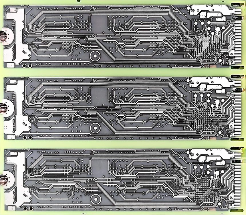
[caption id="attachment_2265" align="alignnone" width="300"]
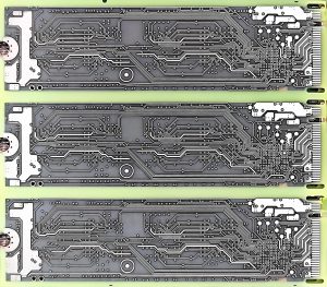
printed circuit board meaning[/caption]
What is a PCB? A Foundation of Connectivity
A PCB (Printed Circuit Board) is much more than a piece of hardware. It’s an intricate network of conductive pathways etched onto a non-conductive material, creating the perfect environment for electrical components to communicate. PCBs are the bridge that connects circuits, enabling them to perform with precision and reliability. Without a PCB, modern electronics would be nothing more than an assortment of disjointed components.
A Marvel of Miniaturization
One of the most impressive feats of PCB technology is its ability to enable miniaturization. As consumer devices, industrial systems, and medical equipment continue to shrink, the demand for smaller, more powerful, and more efficient PCBs increases. Advanced PCB designs allow engineers to pack more functionality into increasingly smaller devices without compromising performance.
For instance, smartphones, once large and cumbersome devices, are now slim, powerful, and feature-packed. The key to this miniaturization is the innovative PCB design, which allows for complex components and intricate circuits to fit into tight spaces, delivering high-speed connectivity and processing power.
Core Components That Bring PCBs to Life
What makes a PCB so unique? Its construction is its strength. From the durable substrate that forms its base to the copper layers carrying electric signals, every element is meticulously crafted to ensure optimal performance. Here’s a breakdown of the essential components:
-
Substrate: The base of a PCB is made from a non-conductive material, typically FR4 (a glass-reinforced epoxy laminate). This material provides strength, rigidity, and thermal stability.
-
Copper Layers: Copper is the material used to create the conductive pathways that connect components. These copper traces are etched onto the PCB’s surface.
-
Solder Mask: The solder mask is a thin layer that protects the copper traces from oxidation and damage while preventing solder bridges during the soldering process.
-
Silkscreen: This layer provides essential markings and labels for components, helping with assembly and troubleshooting.
Together, these components ensure that the PCB operates flawlessly in even the harshest conditions, from industrial environments to consumer gadgets.
Why PCBs Are Indispensable in Modern Electronics
Think of a PCB as the blueprint of innovation. It allows engineers to design increasingly complex devices without compromising on size or efficiency. The precision of PCB layout ensures every connection is optimized for performance, whether in a consumer device or industrial equipment.
Reliability in the Face of Complexity
PCBs are engineered for durability. They withstand heat, vibration, and environmental stress, ensuring that your devices work flawlessly, whether on a factory floor or in the palm of your hand. This reliability is what makes PCBs so valuable in mission-critical applications like aerospace, medical devices, and automotive systems. As devices continue to become more complex, PCBs ensure that everything works in harmony, even under extreme conditions.
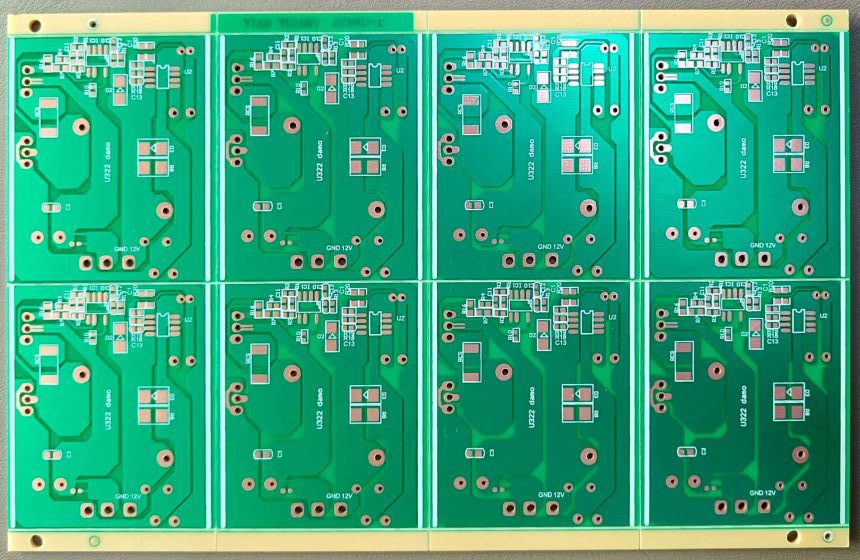
Types of PCBs: A Design for Every Purpose
Not all PCBs are created equal. Simple single-layer boards power small gadgets, while multi-layer boards with dozens of interconnected layers manage the complexities of advanced systems.
-
Single-layer PCBs are the most basic and cost-effective design. They are used in simple devices where the circuit doesn’t need to be very complex.
-
Multi-layer PCBs offer more advanced capabilities, such as the ability to connect multiple circuits through stacked layers. These are common in high-performance devices like smartphones and laptops.
-
Rigid, Flexible, and Rigid-Flex Boards are also critical in the design of cutting-edge devices. Flexible PCBs bend to fit unique designs, while rigid-flex boards combine flexibility with strength, making them ideal for applications in aerospace and medical fields.
For businesses looking for high-quality, reliable PCB solutions, working with a trusted partner like SQPCB ensures that all designs meet the necessary performance and durability standards.
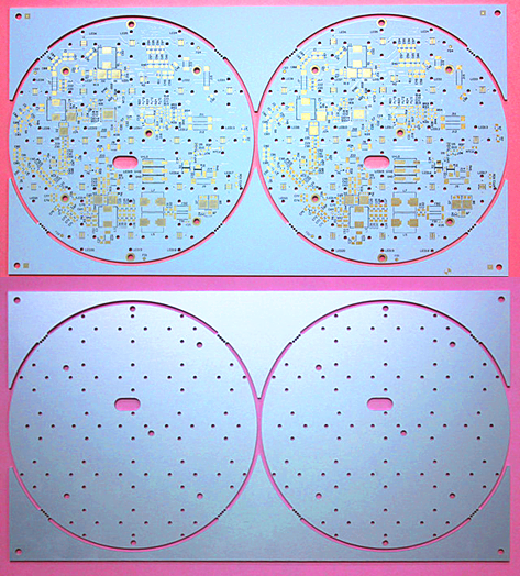
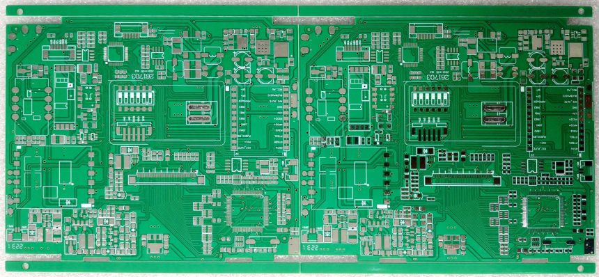
The Art and Science of PCB Manufacturing
Creating a PCB is a journey of precision. Designers use advanced software to craft layouts, while manufacturers employ state-of-the-art machinery to layer, etch, and drill. PCB fabrication requires careful handling at each stage to ensure high-quality outputs, whether for a standard or custom PCB.
From Design to Assembly
The PCB manufacturing process starts with a design phase, where the components are strategically placed to create an efficient circuit. Advanced CAD software is used to design the layout, and photolithography is used to transfer the design onto the PCB. Afterward, the etching process removes unwanted copper to leave behind the circuit pathways.
Once the PCB is fabricated, it goes through assembly, where components are mounted on the board, and connections are made. This step involves techniques like surface-mount technology (SMT) and through-hole technology (THT). The assembled board is then subjected to rigorous testing to ensure it functions correctly.
Testing for Perfection
Before a PCB reaches its final destination, it undergoes rigorous testing. Each trace, each connection, is verified to ensure the board performs without a hitch. A single flaw could render an entire device inoperable, making testing a crucial step in PCB manufacturing.
Common testing methods include Flying Probe Testing for electrical continuity, In-Circuit Testing (ICT) for functional component testing, and Automated Optical Inspection (AOI) to check solder joints and alignment.
Applications: Where printed circuit board meaning Shines
PCBs are used in a wide range of industries, powering everything from consumer electronics to complex industrial machines. Here’s a look at some of the most common applications:
Consumer Electronics
Your smartphone? It’s a marvel of PCB engineering. From managing power to connecting touchscreens, PCBs are at the heart of consumer tech. Custom PCB designs cater to specific product needs, ensuring maximum performance. Companies like SQPCB specialize in designing custom PCBs that meet the specific requirements of consumer electronics.
Automotive and Aerospace
In vehicles, PCBs control navigation systems, sensors, and entertainment units. In aerospace, they withstand extreme conditions to ensure mission success. Flex PCBs are often used in these applications due to their durability and adaptability, allowing the electronics to function reliably even in harsh environments.
Healthcare and Beyond
Medical devices like pacemakers, imaging machines, and monitoring devices rely on PCBs for precision and reliability, proving their critical role in saving lives. The high-performance demands of medical devices require custom-designed PCBs that meet stringent industry standards, something SQPCB excels at.
The Future of PCB: A Revolution in the Making
As technology evolves, so does PCB design. Emerging trends like 3D printing and smart materials are reshaping how the PCB suppliers help to the PCBs created, making them more efficient and sustainable. The integration of PCBs into AI systems and IoT devices promises to revolutionize industries, paving the way for a smarter, more connected future.
Future trends also include embedded components within PCBs to reduce space and improve performance. These innovations are set to make PCBs even more integral to the next generation of electronics.
A Silent Hero Worth Knowing
The next time you pick up your phone or switch on your computer, take a moment to appreciate the humble PCB. Though it works quietly behind the scenes, its impact is monumental. By understanding PCB meaning, what a PCB is, and its role in modern electronics, you gain insight into the very foundation of today’s technological marvels.
Whether you’re looking for custom PCB designs or planning for mass production, partnering with a trusted manufacturer like SQPCB can ensure that your PCBs meet the highest standards of performance and reliability.
FAQ Section
Q1: What is a PCB board?
A PCB (Printed Circuit Board) is a flat board that connects electronic components using conductive pathways etched from copper sheets. It provides structure and electrical connectivity in virtually all modern electronic devices.
Q2: How does the circuit board manufacturing process work?
PCB manufacturing includes multiple stages: design and layout, material selection, layering, etching, drilling, plating, solder mask application, and testing. Each step requires precision machinery and process controls.
Q3: Can I make a PCB board at home?
Yes, for simple prototypes. DIY methods include toner transfer, UV exposure, and chemical etching. However, they are limited in complexity and accuracy compared to industrial manufacturing.
Q4: What materials are used to make a PCB?
Common materials include FR-4 (fiberglass epoxy laminate), copper foil for traces, solder masks, and silkscreen inks. Advanced boards may use ceramics, polyimide, or aluminum substrates.
Q5: How long does it take to manufacture a PCB?
Lead times vary by complexity and volume. Standard boards take 3–7 days, while expedited services offer delivery within 24–72 hours. Complex multilayer boards may require longer.
For all your Easy PCB manufacturing needs, SQPCB is here to assist with high-quality, reliable solutions, whether you're prototyping or scaling production.

 Quote
Quote
 E-mail