Printed Circuit Board Basics: Printed Circuit Boards (PCBs) are the foundation of nearly all electronic devices today, from simple household gadgets to complex industrial machinery. Understanding the basics of PCB design and the process leading up to the final artwork is crucial for anyone involved in electronics design, manufacturing, or repair. This guide will walk you through the essentials, including types of PCBs, the design process, and the creation of final artwork, providing a foundational overview of how PCBs are made and prepared for production.
1. Printed Circuit Board Basics, What is a Printed Circuit Board?
A Printed Circuit Board (PCB) is a thin board made of insulating material, typically fiberglass, onto which conductive pathways are etched. These pathways, also known as traces, connect various components like resistors, capacitors, and transistors, allowing them to work together within a single circuit. PCBs serve as both the structural base and the electrical connector for these components, facilitating the seamless operation of electronic devices.
Printed Circuit Board Basics
PCBs come in various types:
- Single-layer PCBs: Basic type with a single layer of copper. Common in simple electronic devices.
- Double-layer PCBs: Contain two layers of copper, allowing for more complex circuitry.
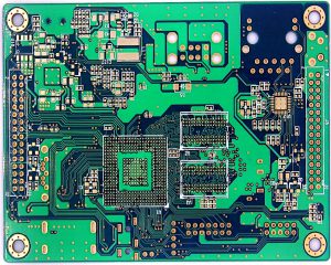
- Multi-layer PCBs: Have multiple layers (usually 4–12) to accommodate intricate circuit designs, commonly used in high-performance electronics.
- Flexible PCBs: Made of flexible materials, allowing for bending and folding, ideal for space-constrained applications.
2. Printed Circuit Board Basics, The PCB Design Process
The design process for PCBs is both an art and a science, involving precision to ensure efficient operation. Here’s an overview of each step:
Step 1: Defining Requirements
Before starting, it’s essential to establish the PCB’s purpose and specifications. This includes deciding on the board’s dimensions, component types, voltage requirements, and specific functionalities needed. Factors like cost, durability, and environmental resistance (e.g., temperature and humidity) are also considered at this stage.
Step 2: Schematic Design
The schematic is a visual representation of the electronic circuit. Engineers use specialized software to create a schematic diagram that shows all components and their connections. Each component has a unique symbol and is linked to others through virtual lines, forming a circuit. This schematic acts as a blueprint for the PCB layout, ensuring that all connections are clear and accurate.
Step 3: PCB Layout Design
Once the schematic is complete, designers move to the PCB layout, where the actual placement of components and traces on the board is determined. Using CAD (Computer-Aided Design) software, they position each component according to the schematic, ensuring efficient use of space and signal flow. Key aspects of the layout design include:
- Component Placement: Arranging components for optimal functionality and ease of manufacturing.
- Trace Routing: Connecting components via conductive traces. Routing can be single-sided, double-sided, or multi-layered, depending on the complexity.
- Power and Ground Planes: Larger copper areas designated for power distribution and grounding, ensuring stable voltage and noise reduction.
- Design Rules Check (DRC): Verifying that the layout complies with electrical and mechanical constraints, such as minimum trace width and component spacing.
3. Creating the Final Artwork
Once the PCB design is completed, it’s time to generate the final artwork, which will serve as a blueprint for manufacturing. This stage involves creating a detailed representation of each PCB layer, including all copper layers, solder masks, and silkscreens.
Step 1: Generating Gerber Files
Gerber files are standard digital files used by PCB manufacturers. Each file represents a different layer of the PCB, including copper layers, solder mask layers, and silkscreen layers. These files are generated through CAD software and include all necessary details for manufacturing.
Step 2: Preparing the Bill of Materials (BOM)
The BOM lists all components used on the PCB, including specific part numbers, quantities, and specifications. This document ensures that the manufacturer uses the correct components during assembly.
Step 3: Design for Manufacturability (DFM) Check
The DFM check ensures that the PCB design is feasible for large-scale production without issues. It involves verifying trace widths, pad sizes, drill hole sizes, and other manufacturing tolerances. This step reduces potential errors and ensures cost-effectiveness.
4. Moving from Final Artwork to Manufacturing
With the Gerber files, BOM, and DFM checks completed, the PCB is ready for production. The manufacturing process typically involves:
- Material Selection: Choosing the base material (such as FR4) and copper type.
- Layer Imaging: Applying the Gerber files to the PCB material via photolithography.
- Etching: Removing excess copper, leaving only the intended circuit traces.
- Drilling and Plating: Creating and plating holes for through-hole components and vias.
- Solder Mask Application: Applying a protective layer that insulates and protects the board.
- Silkscreen Printing: Adding component labels and other visual indicators.
5. Quality Control and Testing
Once the board is assembled, quality control and testing are conducted to verify functionality. Tests include:
- Electrical Testing: Ensures correct connections and no shorts.
- Functional Testing: Verifies that the PCB works as intended in the circuit.
Finally , The journey from a PCB concept to the final artwork is a detailed and systematic process involving design, planning, and meticulous preparation. Each stage, from schematic design to layout and artwork generation, contributes to creating a reliable and functional PCB. By understanding these basics, anyone interested in electronics or engineering can appreciate the complexities and precision that go into PCB production, laying the foundation for innovation in modern electronics.
linkedin sqpcb.com

- long board pcb
- Flexible PCBs
- Special PCB
- Express Printed Circuit Board
- Pcb Prototype
- LED PCB
- PCB
- Printed Circuit Board
- Pcb meaning
- Pcb manufacturer
- Rigid pcb board
- Rigid Flex PCB
 Quote
Quote
 E-mail