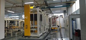
Preventing PCB Warping and Bowing During the Lamination Process
Introduction
PCB warping and bowing are common issues that arise during the lamination process, primarily due to thermal expansion mismatches, resin shrinkage, and internal stress accumulation. During lamination, prepreg (PP), inner layer cores, and copper foil are bonded together at high temperatures (130°C–170°C). As the resin flows and polymerizes, its volume shrinks, and the different materials within the PCB—glass fabric, resin, copper foil, and inner layers—respond to thermal changes differently. If not managed properly, these stresses can lead to permanent board deformation once the PCB returns to room temperature.
To minimize board warping and bowing, manufacturers must optimize the lamination process, material selection, and post-lamination handling techniques. This article explores critical factors and best practices to prevent PCB deformation during lamination.

Preventing PCB Warping and Bowing
Key Considerations to Prevent PCB Warping in Lamination
1. Ensure a Symmetrical Stack-Up Design
- The lamination structure must be symmetrical with respect to the board’s center.
- PP types, copper thickness, and core materials should be as uniform as possible on both sides.
- Asymmetry causes uneven thermal expansion, leading to stress buildup and board warpage.
- If an asymmetrical stack-up is unavoidable, compensation techniques (such as balancing copper distribution) should be applied.
2. Optimize Prepreg Curing Temperature and Time
- Insufficient prepreg curing can lead to re-curing in later production stages, causing additional shrinkage and deformation.
- Ensure the lamination cycle provides enough time and temperature for full resin polymerization.
- Gradual heating and extended dwell time help prevent stress buildup inside the board.
3. Implement Proper Post-Lamination Cooling and Cold Pressing
- After high-temperature lamination, controlled cooling is critical to preventing internal stress.
- Cold pressing after lamination ensures gradual temperature reduction under uniform pressure.
- Rapid or uneven cooling can cause localized contraction, leading to warping.
- Best practice:
- Slow, controlled cooling within the press.
- Maintain uniform pressure during cooling.
- Avoid rapid air cooling that causes non-uniform thermal contraction.
4. Balance Copper Distribution to Minimize Shrinkage Differences
- Uneven residual copper (residual copper ratio) across the board creates thermal expansion and contraction imbalances.
- While inner-layer residual copper is determined by PCB design, outer-layer compensations can help balance stress distribution.
- Solutions to mitigate copper-related warping:
- Use grid or hatch fills in low-copper areas.
- Balance copper density across layers.
- Optimize copper pour distribution for even thermal behavior.
5. Control Material Selection to Reduce Internal Stress
- Modern PCB materials incorporate halogen-free resins and high filler content for environmental and cost reasons.
- These solid fillers improve dimensional stability, helping reduce the risk of warping.
- When selecting materials, ensure:
- High filler content resins for improved warp resistance.
- Prepregs with controlled flow properties to reduce excessive shrinkage.
- Glass fabric with low CTE (Coefficient of Thermal Expansion) for stability.
6. Maintain Proper Prepreg Flow to Prevent Uneven Shrinkage
- Resin flow must match copper thickness and layout density to prevent resin starvation.
- Low-flow prepregs in high-residual-copper areas may lead to voids and weak adhesion, increasing warpage risk.
- Ensure resin flow is optimized for the board’s layout:
- Use higher flow PP in areas with high copper density.
- Avoid excessive resin flow, which can create thickness inconsistencies.
7. Minimize Mechanical Stress in Handling and Cutting
- Improper handling after lamination can introduce additional stress, causing warping.
- Use automated depaneling methods (routing instead of punching) to avoid mechanical deformation.
- Store PCBs flat under controlled humidity and temperature conditions before further processing.
Summary of Best Practices for Preventing PCB Warping
| Factor | Best Practice |
|---|---|
| Stack-Up Symmetry | Ensure symmetrical structure to balance thermal expansion. |
| Prepreg Curing | Fully cure prepreg to prevent post-lamination shrinkage. |
| Cooling & Cold Pressing | Gradual cooling under pressure to release internal stress. |
| Residual Copper Balance | Optimize copper distribution to prevent uneven contraction. |
| Material Selection | Use high-filler resins and stable glass fabric. |
| Prepreg Flow Control | Match resin flow with copper layout to ensure even bonding. |
| Mechanical Stress Reduction | Use gentle handling and stress-free depaneling methods. |
Conclusion
PCB warping and bowing are major challenges in high-layer-count, high-precision circuit boards. By controlling stack-up symmetry, material selection, resin flow, and post-lamination cooling, manufacturers can significantly reduce internal stress and prevent board deformation.
Following optimized lamination processes ensures that PCBs remain flat, stable, and reliable, meeting industry standards for high-speed, HDI, and advanced electronic applications. Implementing these best practices will enhance manufacturing yields, reduce defects, and improve product longevity.
- long board pcb
- Flexible PCBs
- Special PCB
- Express Printed Circuit Board
- Pcb Prototype
- LED PCB
- PCB
- Printed Circuit Board
- Pcb meaning
- Pcb manufacturer
- Rigid pcb board
- Rigid Flex PCB

 Quote
Quote
 E-mail