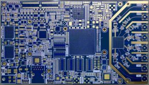
PCB Manufacturing Processes, Printed Circuit Boards (PCBs) are the backbone of modern electronic devices, providing the foundation for electrical connectivity and component support. The manufacturing of PCBs involves a series of complex and precise processes to ensure high quality and reliability. This guide will walk you through the key steps in PCB manufacturing, highlighting best practices and considerations for achieving optimal results.

PCB Manufacturing Processes
Step 1: PCB Manufacturing Processes, Design and Planning
The PCB manufacturing process begins with a detailed design and planning phase. This step involves creating a schematic diagram and laying out the PCB design using computer-aided design (CAD) software. Key considerations include:
- Component Placement: Ensuring efficient and logical placement of components to minimize signal interference and optimize space.
- Routing: Designing trace paths to connect components while avoiding cross-talk and impedance issues.
- Layer Stack-Up: Determining the number of layers and their configuration to meet electrical and mechanical requirements.
Step 2: PCB Manufacturing Processes, Material Selection
Selecting the right materials is crucial for the performance and durability of the PCB. Common materials include:
- Substrate: The base material, typically made of FR4 (fiberglass-reinforced epoxy laminate) for its good electrical insulation and mechanical strength.
- Copper Cladding: Thin layers of copper laminated to the substrate to form conductive traces.
- Solder Mask: A protective layer applied over the copper traces to prevent oxidation and short circuits.
- Silkscreen: A layer used to print component labels, logos, and other markings on the PCB.
Step 3: PCB Manufacturing Processes, Patterning and Imaging
The next step involves transferring the PCB design onto the substrate. This process, known as patterning or imaging, includes:
- Photoresist Application: Coating the substrate with a photosensitive material (photoresist).
- Exposure: Using UV light to expose the photoresist through a photomask, hardening the exposed areas.
- Development: Removing the unexposed photoresist, leaving behind the desired copper pattern.
Step 4: PCB Manufacturing Processes, Etching
Etching is the process of removing unwanted copper from the PCB to reveal the designed circuit pattern. Common etching methods include:
- Chemical Etching: Using chemical solutions (such as ferric chloride or ammonium persulfate) to dissolve the unwanted copper.
- Plasma Etching: A dry etching technique using ionized gases to remove copper, often used for fine-line and high-precision PCBs.
Step 5: PCB Manufacturing Processes, Drilling
Drilling creates holes for component leads, vias (electrical connections between layers), and mounting purposes. Modern PCB manufacturing uses automated drilling machines with high-speed spindles and precision control.
Step 6: PCB Manufacturing Processes, Plating
Plating involves depositing a thin layer of metal (typically copper) onto the drilled holes to create conductive pathways. This step ensures electrical connectivity between different layers of the PCB.
Step 7: PCB Manufacturing Processes, Solder Mask and Silkscreen Application
- Solder Mask: A protective layer applied over the entire PCB surface, except for the pads where components will be soldered. It prevents solder bridging and protects against environmental damage.
- Silkscreen: Printing component labels, reference designators, and other markings on the PCB surface using a contrasting ink.
Step 8: PCB Manufacturing Processes, Surface Finish
The surface finish protects the exposed copper pads and improves solderability. Common surface finishes include:
- HASL (Hot Air Solder Leveling): A layer of solder applied and leveled using hot air.
- ENIG (Electroless Nickel Immersion Gold): A thin layer of gold over nickel, providing excellent solderability and corrosion resistance.
- OSP (Organic Solderability Preservative): A thin, organic layer that protects the copper during storage and assembly.
Step 9: PCB Manufacturing Processes, Assembly
PCB assembly involves mounting and soldering components onto the board. This process includes:
- Pick and Place: Automated machines place components onto the PCB based on the design layout.
- Soldering: Reflow soldering (for surface-mount components) and wave soldering (for through-hole components) to secure the components in place.
Step 10: PCB Manufacturing Processes, Testing and Quality Control
The final step in PCB manufacturing is rigorous testing and quality control to ensure the board functions as intended. Testing methods include:
- Automated Optical Inspection (AOI): Visual inspection using high-resolution cameras to detect defects.
- In-Circuit Testing (ICT): Electrical testing to verify circuit continuity, resistance, and component functionality.
- Functional Testing: Simulating operating conditions to ensure the PCB performs correctly in its intended application.
Conclusion
PCB manufacturing is a meticulous process that requires precision, attention to detail, and advanced technology. From design and material selection to assembly and testing, each step plays a vital role in producing high-quality PCBs. By understanding and implementing best practices in PCB manufacturing, companies like Sqpcb can ensure the reliability and performance of their electronic products.
- long board pcb
- Flexible PCBs
- Special PCB
- Express Printed Circuit Board
- Pcb Prototype
- LED PCB
- PCB
- Printed Circuit Board
- Pcb meaning
- Pcb manufacturer
- Rigid pcb board
- Rigid Flex PCB

 Quote
Quote
 E-mail