Introduction: The Importance of Understanding PCB Layers
In the fast-evolving electronics industry, the structure of a printed circuit board (PCB) significantly impacts device performance, durability, and cost. One of the most critical aspects of PCB design is determining the appropriate number of PCB layers. Whether designing a simple consumer electronic device or a sophisticated aerospace controller, engineers must strategically choose the right layer count to balance electrical performance, space constraints, signal integrity, and cost.
This article explores the methodologies, considerations, and industry best practices used to determine PCB layers, with insights into what manufacturers like SQ PCB offer in terms of support, technology, and reliability. The content integrates both technical detail and strategic thinking, making it ideal for engineers, procurement specialists, and electronics designers.
PCB layers
1. Basic Concepts of PCB Layers
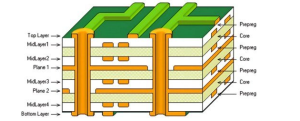
Printed circuit boards come in various configurations, from basic single-layer designs to complex multi-layer stacks exceeding 30 layers. Each layer serves a purpose—signal routing, power distribution, or grounding—and the number of layers chosen directly affects signal integrity, noise management, and thermal behavior.
-
Single-layer PCBs: Suitable for simple devices like calculators or LED panels.
-
Double-layer PCBs: Used in slightly more complex systems like small appliances.
-
Multilayer PCBs: Necessary for high-speed data transmission, signal integrity, and dense component layouts as seen in mobile phones, servers, and medical devices.
2. Key Factors to Consider When Determining PCB Layers
2.1 Signal Integrity Requirements and PCB Layers
High-speed signal transmission demands proper routing, which often necessitates additional layers for ground and power planes. For instance, differential pairs used in USB or HDMI may need at least four layers for proper impedance control and isolation.
2.2 Component Density and PCB Layers
As device complexity increases, so does the number of interconnected components. Designers may be forced to go from a 4-layer to an 8-layer PCB to accommodate additional routing space while maintaining electrical separation.
2.3 Power Distribution Strategy and PCB Layers
More layers allow the separation of high-power and low-power zones and dedicated planes for power distribution. This improves reliability and reduces electromagnetic interference (EMI).
3. How PCB Manufacturers Determine the Number of PCB Layers
Determining PCB layers involves a structured engineering workflow. Here is a generalized outline that PCB manufacturers, including SQ PCB, follow to guide clients:
3.1 Design Review and Requirements Collection
Engineers analyze the schematics, expected current loads, signal speeds, and mechanical constraints of the final product. Power integrity and EMC requirements are also evaluated at this stage.
3.2 Layer Stack-Up Design
The stack-up is defined based on the following:
-
Signal routing requirements
-
Power and ground isolation
-
Dielectric spacing
-
Controlled impedance calculations
Manufacturers like SQ PCB often provide predefined layer stack-up templates for 4, 6, 8, and 10 layers to accelerate prototyping.
3.3 Simulation and Optimization
Before finalizing the PCB layout, simulation tools such as SIwave or HyperLynx are used to evaluate signal integrity, crosstalk, and power distribution across different layer counts.
3.4 Cost vs. Performance Evaluation
An 8-layer board may offer better performance but will cost more than a 4-layer board. Manufacturers assist clients in determining the trade-off that best fits their project scope.
4. Detailed Workflow: From Schematic to Layer Count Selection
4.1 Early Design Planning and PCB Layers
At this phase, engineers define:
-
Maximum board size
-
Required I/O ports
-
Analog/digital zone separation
-
Expected PCB thickness
This sets the stage for estimating the base number of layers.
4.2 Prototyping and Iteration with PCB Layers
Manufacturers such as SQ PCB encourage early prototyping. A common practice is to begin with 4 layers, test functionality, and then upscale if signal degradation or heat issues are observed.
5. Common Layer Stack-Up Configurations
Here are some widely adopted stack-up structures for standard applications:
| Layers | Common Stack-up | Application |
|---|---|---|
| 2-layer | Signal / Ground-Power | Basic controllers, small appliances |
| 4-layer | Signal / Ground / Power / Signal | Consumer electronics, wearables |
| 6-layer | Signal / Ground / Power / Ground / Signal | Industrial controls, automotive |
| 8-layer | Signal / Ground / Power / Signal / Signal / Power / Ground / Signal | Telecom, medical devices |
6. Industry Case Studies on Choosing PCB Layers
6.1 Case Study: Wearable Health Device
Design engineers initially planned a 2-layer board. However, interference between analog sensors and digital communication lines required separation with ground planes—necessitating a shift to a 4-layer board.
6.2 Case Study: Automotive Radar System
Starting with a 6-layer configuration, the team had to scale to 10 layers due to:
-
High-speed CAN bus requirements
-
EMI constraints
-
Shielding needs
The manufacturer’s simulation support played a critical role in optimizing the layout.
7. Common Mistakes in Determining PCB Layers
-
Underestimating EMI issues: Trying to keep layer count low while compromising noise immunity.
-
Over-designing: Adding unnecessary layers “just in case,” resulting in bloated costs.
-
Ignoring manufacturability: Designing complex layer stack-ups incompatible with mass-production equipment.
SQ PCB helps clients mitigate these issues by offering consultative design-for-manufacturing (DFM) reviews during early phases.
8. Personal Insights: Strategic Thinking in Layer Selection
From a practical standpoint, the temptation to minimize cost often leads engineers to restrict themselves to 2-layer or 4-layer designs. But this can be short-sighted. In today’s fast-switching environments and tightly packed enclosures, strategic investment in additional layers pays off in reduced EMI, simplified routing, and better thermal balance.
Also, with vendors like SQ PCB offering competitive pricing for 6–10 layer boards, the cost gap is not as prohibitive as it once was. More importantly, better design choices reduce debugging time and field failures—both of which are significantly more expensive in the long run.
9. Advanced Techniques to Optimize PCB Layers
9.1 Blind and Buried Vias in PCB Layers
One of the most effective ways to optimize layer usage is by incorporating blind and buried vias:
-
Blind vias connect outer layers to inner layers without going through the entire PCB.
-
Buried vias connect internal layers and are invisible from the surface.
These allow for denser routing without adding more PCB layers. However, they increase manufacturing complexity and cost. When used strategically, they help reduce layer count while preserving high-density routing.
9.2 Via-in-Pad Technology and PCB Layers
Via-in-pad technology places vias directly under component pads (such as BGAs). This enables more compact layouts and can sometimes reduce the need for extra layers. While this technique is common in high-frequency and miniaturized applications, it demands precise manufacturing capabilities, such as those offered by SQ PCB.
10. High-Speed Design Considerations in Multilayer PCB Layers
10.1 Controlled Impedance and PCB Layers
High-speed signals (e.g., USB 3.0, PCIe, DDR) require controlled impedance routing. This is typically achieved with at least four PCB layers:
-
Top: signal
-
Inner 1: ground
-
Inner 2: power
-
Bottom: signal
This configuration ensures consistent impedance, which is crucial for preventing reflections and signal degradation.
10.2 Crosstalk Reduction Using Additional PCB Layers
As signal frequencies increase, the risk of crosstalk between traces rises. Adding extra ground layers between signal layers effectively isolates signals, improving noise immunity.
10.3 Power Integrity in High-Speed PCB Layers
Designers must provide robust and low-impedance power paths. This usually requires dedicated power planes, contributing to higher PCB layer counts. For example, in a 10-layer board, two layers may be exclusively reserved for power distribution.
Conclusion: Mastering PCB Layer Decisions for Success
Determining the number of PCB layers is not just a technical decision—it’s a strategic one. From cost and performance to manufacturability and product lifecycle, the number of layers in your board design influences nearly every aspect of the final product.
By understanding the functional role of each layer, leveraging best practices in layout and simulation, and working with a capable manufacturer like SQ PCB, design teams can make confident, informed decisions. As electronics become smaller, faster, and more complex, mastering PCB layer strategy becomes not just advantageous—but essential.
Frequently Asked Questions (FAQs)
FAQ 1: What is the difference between rolled copper foil and electrolytic copper foil?
Answer: Rolled copper foil is produced by mechanically rolling copper into thin sheets, offering better surface quality and mechanical strength. Electrolytic copper foil is deposited via an electrolytic process and is more flexible and cost-effective.
FAQ 2: How do I know when to switch from 2-layer to 4-layer PCB?
Answer: When signal integrity, EMI, or power routing becomes a concern, especially in high-speed or analog/mixed-signal designs, it’s advisable to upgrade to at least a 4-layer stack-up.
FAQ 3: Can I reduce PCB layers after simulation?
Answer: Yes, simulation often reveals overengineering. If signal performance is satisfactory, you can reduce layer count to save costs, but only after thorough verification.
FAQ 4: How does PCB thickness affect the number of layers?
Answer: Thicker PCBs can accommodate more layers but may introduce mechanical and thermal constraints. Some high-layer-count PCBs use thinner dielectric materials to maintain overall board thickness within spec.
FAQ 5: Is there a maximum number of layers for a PCB?
Answer: While there’s no strict upper limit, practical manufacturing constraints usually cap layer counts at 30–40 for standard vendors. High-layer-count PCBs are mostly used in military or supercomputing applications.

- long board pcb
- Flexible PCBs
- Special PCB
- Express Printed Circuit Board
- Pcb Prototype
- LED PCB
- PCB
- Printed Circuit Board
- Pcb meaning
- Pcb manufacturer
- Rigid pcb board
- Rigid Flex PCB
 Quote
Quote
 E-mail