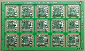
PCB inspection is an essential step in the electronics manufacturing process, ensuring that printed circuit boards (PCBs) are free from defects before they are used in final products. This process plays a vital role in ensuring product quality and reliability, particularly for high-precision devices. In this article, we’ll dive deep into the various techniques used in PCB inspection, their benefits, and the best practices for ensuring that your PCB production runs smoothly, with minimal defects.
PCB Inspection
1. The Importance of PCB Inspection
PCB inspection is critical in ensuring the functionality and reliability of the final product. Whether you’re dealing with high-speed circuits, consumer electronics, or automotive systems, inspecting the PCB ensures that the components are placed correctly and that the circuit is free of faults. Without proper inspection, the risks of defective circuits, malfunctioning devices, and costly product recalls can skyrocket.
But here’s the kicker: PCB inspection doesn’t just prevent failures; it also increases manufacturing efficiency. By catching defects early, manufacturers can reduce the need for rework and optimize their production processes. The stakes are high when it comes to PCB inspection, as even a small flaw in a PCB can cause a cascade of issues in the final product. Effective inspection improves yield, ensures quality control, and ultimately leads to more reliable electronics.
PCB inspection can be done at various stages of production, including during the assembly process, after soldering, and before shipment. The goal is to catch any defects or issues that might compromise the performance of the PCB.
Table 1: Key Benefits of PCB Inspection
| Benefit | Description | Impact on Production |
|---|---|---|
| Quality Assurance | Ensures the final product meets design specs | Reduces defects and increases reliability |
| Cost Efficiency | Identifies defects early to reduce rework | Lowers production costs |
| Manufacturing Speed | Speeds up production by reducing defects | Increases throughput and efficiency |
2. Types of PCB Inspection Methods
There are various methods of PCB inspection, each suited for different types of defects and production processes. From manual visual inspections to fully automated systems, each method plays an important role in ensuring the reliability of the final product.
What’s the real story? Each inspection method has its own advantages and limitations. By understanding the strengths and weaknesses of each approach, manufacturers can select the right inspection techniques for their specific needs. Let’s explore some of the most common methods:
- Visual Inspection: This is the most basic and traditional method, where trained operators visually inspect the PCB for defects such as misplaced components, soldering issues, and physical damage. While effective for simple PCBs or low-volume production, visual inspection can be time-consuming and prone to human error.
- Automated Optical Inspection (AOI): AOI uses cameras and software to detect defects such as misaligned components, solder bridges, or missing components. It’s faster and more accurate than visual inspection, especially for high-density boards.
- X-ray Inspection: X-ray inspection is used to inspect multi-layer PCBs and hidden solder joints that are not visible on the surface. This method is especially useful for detecting defects in BGA (Ball Grid Array) packages, which are impossible to inspect visually.
- Electrical Testing: Electrical testing checks the functionality of the PCB by testing for shorts, opens, and other electrical defects. This method ensures that the circuit operates correctly before moving to the final assembly stage.
Table 2: Comparison of PCB Inspection Methods
| Inspection Method | Key Features | Best Use Case |
|---|---|---|
| Visual Inspection | Manual check for visible defects | Low-volume production or simple boards |
| AOI (Automated Optical Inspection) | Uses cameras and software for defect detection | High-density PCBs, high-volume production |
| X-ray Inspection | Inspects hidden defects using X-rays | Multilayer PCBs, BGAs, and hidden solder joints |
| Electrical Testing | Tests for electrical faults like shorts and opens | Ensures functionality of the PCB |
3. Visual Inspection in PCB Manufacturing
Visual inspection is the oldest and simplest method of PCB inspection. It involves manually inspecting the board to identify defects such as component misalignment, incorrect soldering, and physical damage to the PCB. Despite its simplicity, visual inspection is still widely used, particularly in low-volume or early-stage production.
Ready for the good part? While visual inspection is crucial for identifying large-scale or visible defects, its effectiveness can be limited by human error, fatigue, and the complexity of the board design. However, when combined with other inspection methods, it becomes a powerful tool in the PCB quality control process.
- Manual Inspection: In manual visual inspection, workers check each PCB for visible defects. This method is cost-effective but can be slow and prone to inconsistency.
- Benefits of Visual Inspection: Visual inspection allows operators to catch simple mistakes, such as misplaced components, poor solder joints, or cracked PCBs. It’s quick and inexpensive for smaller batches.
- Limitations of Visual Inspection: The method is prone to fatigue, especially for operators who must inspect hundreds or thousands of PCBs. Additionally, it can’t identify internal defects or problems in smaller components.
Table 3: Pros and Cons of Visual Inspection
| Advantage | Description | Disadvantage |
|---|---|---|
| Cost-Effective | Low cost of implementation | Subject to human error and fatigue |
| Easy to Implement | Simple process, easy for operators to follow | Limited to visible defects only |
| Speed | Quick for small quantities of PCBs | Time-consuming for high-volume production |
4. Automated Optical Inspection (AOI)
AOI uses high-resolution cameras and advanced software to inspect PCBs for defects like misalignment, missing components, soldering issues, and surface damage. It’s an automated process that can inspect many PCBs in a short amount of time, making it ideal for high-volume production.
What’s the real story? AOI is faster, more accurate, and less prone to human error than visual inspection. It’s also capable of detecting very small defects that might be missed by the human eye. However, AOI is not perfect—it may still struggle with certain types of defects, such as underfilled solder joints or very fine traces.
AOI works by capturing images of the PCB and comparing them to a pre-programmed design file to check for discrepancies. If any defects are found, the system will alert operators, who can then address the issue before proceeding.
- AOI Applications: AOI is often used in high-density boards where defects may be too small for manual inspection. It’s also ideal for detecting defects in areas where visual inspection would be difficult.
- Benefits of AOI: The main benefits include faster inspection times, improved consistency, and the ability to handle large production volumes.
- Limitations of AOI: AOI may not detect all types of defects, such as internal layer issues in multi-layer boards. It also requires calibration and regular maintenance to remain effective.
Table 4: Advantages and Limitations of AOI
| Advantage | Description | Limitation |
|---|---|---|
| Fast and Efficient | Can inspect a large number of PCBs quickly | Limited to surface-level defects |
| High Accuracy | Detects small and subtle defects | Can miss underfilled solder joints or fine traces |
| Consistent Results | Reduces human error | Requires regular calibration and maintenance |
5. X-ray Inspection in PCB Testing
X-ray inspection is an advanced technique used to inspect multi-layer PCBs and hidden components, such as BGA and flip-chip packages, which cannot be easily checked with traditional methods. X-ray machines send high-frequency X-rays through the PCB to capture detailed images of the internal layers and components.
Ready for the good part? X-ray inspection is invaluable for detecting defects in complex, high-performance boards, particularly in industries like automotive, medical, and telecommunications. It provides a level of insight that other methods simply cannot.
- How X-ray Works: X-ray inspection captures cross-sectional images of the PCB, revealing hidden solder joints, component placement, and internal wiring. The images are then analyzed for defects.
- Applications: It’s ideal for inspecting hidden solder joints in BGA packages, detecting voids in solder balls, and examining internal layer connections in multi-layer PCBs.
- Advantages: X-ray inspection allows manufacturers to verify that components are correctly soldered, even in tightly packed, multilayered designs. It is essential for detecting issues that are not visible to the naked eye.
- Limitations: X-ray inspection is expensive, requiring specialized equipment and training. It is also slower than AOI and may not be suitable for high-volume production.
Table 5: Pros and Cons of X-ray Inspection
| Advantage | Description | Limitation |
|---|---|---|
| Detects Hidden Defects | Can inspect internal solder joints and connections | Expensive equipment and slow processing time |
| High Accuracy | Provides detailed internal images | Requires skilled operators and regular maintenance |
| Suitable for Complex PCBs | Ideal for multilayer boards and BGAs | Not suitable for low-volume production |
6. Electrical Testing for PCBs
Electrical testing checks whether the PCB is functioning as intended by evaluating its electrical connectivity. This method involves using automated equipment to test for shorts, opens, and other electrical faults. Electrical testing is an essential part of the PCB inspection process, particularly for ensuring that a board will perform correctly in its final application.
What’s the real story? Electrical testing ensures that every connection on a PCB works as designed. It’s one of the most reliable ways to detect problems that other inspection methods might miss, such as faulty traces, improper connections, or short circuits.
- Types of Electrical Tests: The most common electrical tests include continuity testing, which checks for open or short circuits, and in-circuit testing (ICT), which tests the components on the board in place.
- Benefits: Electrical testing is highly reliable for detecting electrical faults that would affect the PCB’s performance. It also helps in verifying that the components are properly placed and soldered.
- Limitations: Electrical testing is only useful for detecting electrical defects, not for visual issues or physical damage like broken components or poor soldering.
Table 6: Types of Electrical Testing
| Test Type | Description | Use Case |
|---|---|---|
| Continuity Testing | Checks for open circuits and shorts | Verifies electrical paths and connections |
| In-Circuit Testing | Tests components while still on the PCB | Verifies component functionality and placement |
| Functional Testing | Ensures the PCB operates as intended in its final application | Confirms overall performance and reliability |
7. Conclusion
PCB inspection is essential for ensuring that electronic products are functional, reliable, and free from defects. By employing a combination of visual inspection, AOI, X-ray inspection, and electrical testing, manufacturers can catch defects early in the production process, ensuring that only high-quality PCBs reach the market. The right inspection method, coupled with best practices, can help save time, reduce costs, and prevent product failures.
FAQ
Q1: What is PCB inspection?
PCB inspection is the process of checking printed circuit boards for defects, ensuring they meet design specifications and quality standards.
Q2: How does Automated Optical Inspection (AOI) work?
AOI uses cameras and specialized software to automatically check PCBs for visual defects such as misalignments, missing components, or soldering issues.
Q3: What is the difference between visual inspection and X-ray inspection?
Visual inspection involves manually or optically inspecting the board, while X-ray inspection allows for the detection of hidden defects in multilayer PCBs that are not visible from the surface.
Q4: Why is electrical testing important for PCB inspection?
Electrical testing checks the functionality of the PCB by verifying circuit connectivity, ensuring that there are no short circuits or open circuits.
Q5: How can I improve the efficiency of PCB inspection in my facility?
Improving efficiency involves using automated inspection methods, training staff on best practices, maintaining equipment regularly, and ensuring compliance with industry standards.

- long board pcb
- Flexible PCBs
- Special PCB
- Express Printed Circuit Board
- Pcb Prototype
- LED PCB
- PCB
- Printed Circuit Board
- Pcb meaning
- Pcb manufacturer
- Rigid pcb board
- Rigid Flex PCB
 Quote
Quote
 E-mail