What is PCB ICD Issure: Inner Connection Defects
Introduction
In the world of printed circuit boards (PCBs), reliability and performance are critical factors that determine the success of any electronic product. One of the major challenges that manufacturers face is ensuring the integrity of internal connections within multilayer PCBs. Inner Connection Defects (ICD) are one of the most critical failure points in PCB manufacturing, and they can significantly impact the performance, durability, and overall quality of electronic products. This article will explore the causes, types, detection methods, and preventive measures related to ICDs in PCB manufacturing.
PCB ICD Issure
What is PCB ICD (Inner Connection Defects)?
Inner Connection Defects (ICD) refer to failures or irregularities that occur in the internal layers of a PCB, particularly in the interconnections between different layers. These defects can be caused by various manufacturing issues such as poor drilling, contamination, inadequate plating, or thermal stress during assembly. Since modern electronic devices rely on high-density interconnect (HDI) and multilayer PCBs, PCB ICDs pose a significant challenge, as they are not easily visible or detectable without advanced inspection techniques.
PCB ICDs can lead to serious problems, such as:
- Electrical failures due to broken or weak internal connections.
- Increased resistance in circuits, leading to excessive heat generation.
- Reduced mechanical strength of vias, resulting in delamination.
- Short circuits or open circuits, leading to system failures in electronic devices.
Causes of ICD in PCB Manufacturing
There are multiple causes of ICD in PCB production, most of which are related to manufacturing processes. Below are some of the most common reasons:
1. Poor Drilling Process
- The process of drilling holes in PCB ICDs must be precise, especially for via connections. If the drilling speed, pressure, or tool quality is not properly controlled, it can result in rough via walls, micro-cracks, or inconsistencies in hole size.
- Improper drilling can lead to hole wall defects, which cause poor adhesion of the plating material, weakening the connection between layers.
2. Contamination or Foreign Material
- The presence of contaminants such as dust, debris, or oxidation can prevent proper adhesion of conductive layers during plating.
- Contamination in plating solutions may cause voids or weak adhesion, leading to potential open circuits or intermittent failures.
3. Insufficient or Poor Electroplating
- Electroplating defects occur when the copper deposition inside vias or holes is too thin or uneven, creating weak points in the connection.
- Poor copper plating can lead to voids, cracks, or weak mechanical strength, making the PCB susceptible to failure under stress.
4. Thermal Stress and Expansion
- PCBs undergo thermal cycling during assembly and use. If the materials used in the PCB do not have matching coefficients of thermal expansion (CTE), internal layers may expand at different rates, leading to delamination or cracks in the plated-through holes (PTHs).
- Over time, repeated thermal cycles can cause copper fatigue, leading to connection failure.
5. Improper Lamination Process
- If the lamination process is not carefully controlled, it can lead to delamination or improper bonding between layers.
- Poor lamination may create air gaps or voids, reducing electrical conductivity and mechanical strength.
6. Manufacturing Process Variability
- Inconsistent process parameters, such as variations in drilling speed, plating current, or temperature control, can introduce fluctuations in PCB quality, leading to inner connection defects.
- Even small variations in etching, pressing, or chemical processes can significantly impact PCB reliability.
Types of Inner Connection Defects (ICD)
There are different types of ICDs that can occur in a multilayer PCB. The most common types include:
1. Barrel Cracks
- These are fractures in the plated hole walls caused by mechanical stress or poor plating.
- Barrel cracks can result in intermittent or permanent electrical failures.
2. Inner Layer Separation
- This occurs when the inner copper layers lose their connection due to poor bonding or thermal expansion.
- Inner layer separation can cause high resistance or complete loss of connectivity.
3. Plating Voids
- Plating voids refer to gaps or unplated areas in the via wall caused by poor electroplating or contamination.
- These voids weaken the structural integrity of the via and lead to open circuits or reduced current capacity.
4. Micro-Cracks and Delamination
- Micro-cracks are tiny fractures in the copper plating that develop due to thermal cycling or mechanical stress.
- Delamination occurs when layers separate due to weak adhesive bonds or excessive heat exposure.
5. Copper Thin-Out or Etching Defects
- Over-etching or under-plating of copper layers can lead to uneven current flow, which may cause overheating and failure in high-power applications.
How to Detect ICD in PCBs?
Since inner connection defects are not visible to the naked eye, specialized testing methods are required to detect them. Some of the most commonly used inspection techniques include:
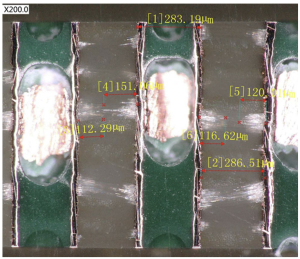
1. Cross-Sectional Analysis
- This method involves cutting a sample PCB and examining the internal layers under a microscope to identify cracks, voids, and separation.
2. X-ray Inspection
- X-ray technology allows manufacturers to see inside the PCB layers and identify internal defects without cutting the board.
3. Electrical Testing (Continuity and Resistance Checks)
- Continuity tests check if electrical signals pass through all required connections.
- Resistance measurements can help detect high-resistance joints or weakened vias.
4. Thermal Cycling and Stress Testing
- Thermal cycling tests expose PCBs to extreme temperatures to check for cracks or delamination under stress.
5. Time-Domain Reflectometry (TDR)
- This advanced technique measures the impedance of PCB traces and detects open circuits, short circuits, and impedance mismatches caused by ICDs.
How to Prevent Inner Connection Defects?
To ensure high-quality PCBs and prevent ICDs, manufacturers must follow strict quality control measures and optimize production processes. Some key preventive measures include:
1. Improve Drilling Accuracy
- Use high-precision drilling machines and optimize drilling parameters to minimize defects in via walls.
2. Enhance Plating Quality
- Implement strict electroplating control, ensuring uniform copper deposition with the right thickness.
3. Use High-Quality Materials
- Select PCB materials with matching thermal expansion properties to prevent delamination and cracking.
4. Perform Rigorous Quality Testing
- Use advanced X-ray and electrical testing to identify defects before final assembly.
5. Optimize the Lamination Process
- Ensure uniform heat and pressure distribution during lamination to avoid air gaps and weak adhesion.
6. Regular Process Monitoring and Auditing
- Continuously monitor manufacturing conditions, and conduct frequent audits to maintain consistent production quality.
Conclusion
Inner Connection Defects (PCB ICD) are one of the most critical issues in multilayer PCB manufacturing, affecting reliability, electrical performance, and mechanical strength. Understanding the root causes, identifying potential defects through rigorous testing, and implementing strict quality control measures are key to preventing these issues. With advancements in inspection technologies and improved manufacturing processes, the industry can continue to enhance PCB reliability and performance, ensuring the successful operation of modern electronic devices.

- long board pcb
- Flexible PCBs
- Special PCB
- Express Printed Circuit Board
- Pcb Prototype
- LED PCB
- PCB
- Printed Circuit Board
- Pcb meaning
- Pcb manufacturer
- Rigid pcb board
- Rigid Flex PCB
 Quote
Quote
 E-mail