Comparison of PCB Exposure Machines: Manual Alignment, CCD Semi-Automatic, CCD Fully Automatic, and DI Exposure Machines
Introduction
In PCB (Printed Circuit Board) manufacturing, exposure machines play a crucial role in transferring circuit patterns onto photoresist-coated substrates. Various exposure machines are available, ranging from manual alignment exposure machines to advanced Direct Imaging (DI) exposure systems. The choice of equipment significantly impacts production efficiency, alignment precision, defect rates, and overall manufacturing costs.
This article compares four major types of PCB exposure machines: Manual Alignment Exposure Machine, CCD Semi-Automatic Exposure Machine, CCD Fully Automatic Exposure Machine, and DI Exposure Machine. We will evaluate their working principles, accuracy, efficiency, cost, and suitability for different production environments.
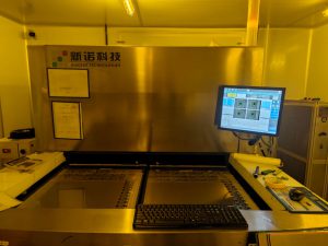
PCB Exposure Machine
Overview of PCB Exposure Machines
| Machine Type | Alignment Method | Production Speed | Accuracy | Cost | Best for |
|---|---|---|---|---|---|
| Manual Alignment Exposure Machine | Hand-adjusted | Slow | Low (Operator-dependent) | Low | Prototyping, small-scale production |
| CCD Semi-Automatic Exposure Machine | CCD-assisted manual alignment | Medium | Moderate | Medium | Small to mid-volume production |
| CCD Fully Automatic Exposure Machine | CCD automatic alignment | Fast | High | High | High-volume mass production |
| DI (Direct Imaging) Exposure Machine | Laser direct imaging (no film required) | Fastest | Ultra-High | Very High | High-precision HDI and high-layer count PCBs |
1. Manual Alignment Exposure Machine
Working Principle
- The operator manually aligns phototool films with the PCB substrate before UV exposure.
- Positioning is adjusted by hand, requiring skilled labor for accuracy.
- Exposure occurs using high-intensity UV light to transfer the circuit pattern onto the photoresist-coated PCB.
Advantages
✅ Low Cost – Requires minimal investment, making it suitable for small factories and startups. ✅ Simple Operation – Does not require complex software or calibration. ✅ Ideal for Prototyping – Suitable for low-volume, experimental, or one-off PCB production.
Disadvantages
❌ Low Accuracy – Alignment errors are operator-dependent, leading to higher defect rates. ❌ Slow Process – Manual positioning and adjustments take significantly longer than automated systems. ❌ Limited for Mass Production – Not suitable for high-volume manufacturing due to inconsistency and speed limitations.
2. CCD Semi-Automatic Exposure Machine
Working Principle
- Utilizes CCD cameras to assist in alignment but still requires manual adjustments.
- The operator positions the PCB, and the CCD system provides visual guidance for alignment.
- Once aligned, UV exposure is automatically executed.
Advantages
✅ Improved Accuracy – CCD cameras reduce human alignment errors, increasing yield rates. ✅ Faster than Manual Exposure – Speeds up production compared to manual alignment. ✅ Moderate Cost – More affordable than fully automated exposure machines.
Disadvantages
❌ Still Requires Manual Input – Operator skill is still a factor, limiting repeatability. ❌ Not Fully Automated – Some time is lost in manual adjustments, making it less efficient for mass production.
3. CCD Fully Automatic Exposure Machine
Working Principle
- Uses CCD cameras and an automated positioning system to precisely align phototools with the PCB.
- Once the PCB is loaded, the system automatically aligns and exposes it without manual intervention.
- High-speed UV exposure ensures consistent imaging.
Advantages
✅ High Precision Alignment – Achieves extremely low misalignment rates, improving PCB quality. ✅ Fast Production Speed – Ideal for mass production where efficiency is critical. ✅ Consistent Repeatability – Eliminates operator-dependent errors.
Disadvantages
❌ Higher Cost – Requires a larger investment, making it suitable for medium to large-scale manufacturers. ❌ Complex Setup and Maintenance – Requires trained personnel for operation and maintenance.
4. DI (Direct Imaging) Exposure Machine
Working Principle
- No phototool film is required; instead, a laser directly exposes the photoresist.
- Uses computer-controlled laser beams to transfer circuit patterns onto the PCB with ultra-high precision.
- Suitable for fine-line PCBs, HDI designs, and quick prototyping.
Advantages
✅ Ultra-High Precision – Best for fine-pitch circuits and HDI PCBs. ✅ No Phototool Films Needed – Eliminates film alignment errors and maintenance costs. ✅ Fast Processing – Speeds up production by reducing setup time. ✅ Great for Quick Turnaround and Prototyping – Ideal for small-batch, high-precision PCB manufacturing.
Disadvantages
❌ Very High Cost – Initial investment is expensive, limiting use to high-end manufacturing facilities. ❌ Requires Special Photoresist – Only works with DI-compatible resists, adding material constraints. ❌ Not Suitable for Low-End Production – Overkill for simple, low-density PCBs.
Cost Comparison
| Machine Type | Relative Cost (Manual = 1) |
| Manual Alignment Exposure Machine | 1.0 |
| CCD Semi-Automatic Exposure Machine | 3.0 – 5.0 |
| CCD Fully Automatic Exposure Machine | 6.0 – 10.0 |
| DI Exposure Machine | 15.0 – 25.0 |
- Manual machines are the most affordable but have high defect rates.
- CCD-assisted machines provide better accuracy while remaining cost-effective.
- DI exposure machines are the most expensive but are essential for high-end PCB fabrication.
Conclusion: Choosing the Right Exposure Machine
- For Prototyping or Small-Scale Production → Manual Exposure Machines
- For Cost-Effective Medium Production → CCD Semi-Automatic Exposure Machines
- For High-Speed Mass Production → CCD Fully Automatic Exposure Machines
- For HDI, Fine-Pitch, and High-End PCBs → DI Exposure Machines
Each exposure machine has its strengths and weaknesses, and the right choice depends on production volume, precision requirements, and budget. While manual machines remain relevant for low-cost applications, CCD-assisted and DI exposure technologies are now the standard for high-end, high-precision PCB manufacturing.
By investing in advanced exposure equipment, manufacturers can reduce defects, improve efficiency, and maintain high-quality PCB production standards in today’s demanding electronics industry.
our linkedin sqpcb.com

- long board pcb
- Flexible PCBs
- Special PCB
- Express Printed Circuit Board
- Pcb Prototype
- LED PCB
- PCB
- Printed Circuit Board
- Pcb meaning
- Pcb manufacturer
- Rigid pcb board
- Rigid Flex PCB
 Quote
Quote
 E-mail