Introduction to PCB Delamination
PCB delamination, a critical failure mode in printed circuit board (PCB) manufacturing, occurs when the layers of a PCB separate due to weakened adhesion between materials. This defect compromises structural integrity, electrical performance, and long-term reliability, especially in harsh environments. From consumer electronics to aerospace systems, PCB delamination poses significant risks if not properly addressed. This guide explores the root causes, detection methods, and advanced strategies to mitigate PCB delamination, ensuring robust and durable PCB designs.
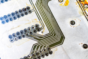
Delamination is a type of damage that can occur to a printed circuit board. It results in the layers of the base material separating from one another. The process is easy to identify because the board will have small, visible gaps or bubbles, typically referred to as blisters.
They occur if the laminate on the base material is exposed to humidity. Heating during the production process turns the humidity into a gas, causing blistering and layer movement.
PCBs consist of multiple layers. The base materials typically consist of FR-4, a laminate material made from woven fiberglass. A flame-resistant, epoxy resin binds these FR-4 layers. During delamination, heat and humidity either loosen the resin from the fiberglass or loosen the resin from the foil or laminate.
Delamination occurs in two distinct steps. Adhesive failure occurs first. As the resin loosens and disintegrates, the blisters appear. Next, the boards move apart, as they’re no longer bound by adhesive. It has a cumulative effect: As the boards shift position, they put pressure on the already-weak adhesive, resulting in additional separation.
Once delamination begins, a few remedies are possible, but they’re not guaranteed. Instead, most anti-delamination efforts focus on prevention. Delamination is almost always the result of issues on the production side. The most effective solutions against delamination are batch testing, high-quality materials, and controlled production methods.
PCB delamination refers to the separation of copper layers, prepreg, or core materials within a PCB stackup. It often manifests as bulges, voids, or cracks, leading to intermittent connections or catastrophic failures.
1. Causes of PCB Delamination
1.1 Material-Related Causes of PCB Delamination
The materials used in PCB fabrication significantly influence the board’s susceptibility to delamination. Key material-related causes include:
-
Moisture Absorption: PCBs can absorb moisture from the environment, which, when subjected to high temperatures during manufacturing processes like soldering, can vaporize and cause internal stresses leading to delamination.
-
Substandard Laminates: Using low-quality or incompatible laminate materials can result in poor adhesion between layers, increasing the risk of delamination.
-
Inadequate Resin Content: Insufficient resin in the laminate can lead to weak bonding between layers, making the PCB more prone to separation under stress.
1.2 Process-Induced Causes of PCB Delamination
Manufacturing processes play a crucial role in the integrity of PCBs. Process-induced causes of delamination include:
-
Thermal Stress: Sudden temperature changes during processes like reflow soldering can induce thermomechanical stress, potentially causing delamination.
-
Drilling Defects: Improper drilling techniques can create micro-cracks or rough hole walls, which can act as initiation points for delamination.
-
Inadequate Curing: Insufficient curing of the laminate materials can result in incomplete polymerization, leading to weak interlayer bonds.
1.3 Environmental Factors Leading to PCB Delamination
External environmental conditions can also contribute to PCB delamination:
-
Humidity Exposure: High humidity environments can lead to moisture absorption by the PCB, increasing the risk of delamination during thermal processing.
-
Chemical Exposure: Contact with harsh chemicals during manufacturing or operation can degrade laminate materials, weakening interlayer bonds.
-
Mechanical Stress: Physical stresses such as bending or vibrations during assembly or operation can initiate or propagate delamination.
PCB Delamination
2. Effects of PCB Delamination
2.1 Electrical Implications of PCB Delamination
Delamination can severely impact the electrical performance of a PCB:
-
Open Circuits: Separation of conductive layers can interrupt electrical pathways, leading to open circuits.
-
Short Circuits: Delaminated layers may cause unintended connections between conductive traces, resulting in short circuits.
-
Impedance Variations: Changes in the dielectric properties due to delamination can alter the impedance of transmission lines, affecting signal integrity.
2.2 Mechanical Consequences of PCB Delamination
The mechanical integrity of a PCB is compromised by delamination:
-
Structural Weakness: Delamination reduces the mechanical strength of the PCB, making it more susceptible to bending or breaking.
-
Component Detachment: Weakened adhesion between layers can lead to the detachment of surface-mounted components.
2.3 Thermal Management Issues Due to PCB Delamination
Effective thermal management is crucial for PCB reliability:
-
Hot Spots: Delaminated areas can impede heat dissipation, leading to localized overheating.
-
Thermal Runaway: Accumulation of heat in delaminated regions can exacerbate material degradation, potentially leading to thermal runaway conditions.
3. Detection and Testing Methods for PCB Delamination
3.1 Visual Inspection for PCB Delamination
Visual inspection is a fundamental method for detecting delamination:
-
Surface Anomalies: Visible signs such as blisters, bubbles, or discoloration on the PCB surface can indicate delamination.
-
Microscopic Examination: High-magnification inspection can reveal micro-cracks or layer separations not visible to the naked eye.
3.2 Non-Destructive Testing (NDT) Techniques for PCB Delamination
Advanced NDT methods allow for internal inspection without damaging the PCB:
-
Scanning Acoustic Microscopy (SAM): Utilizes high-frequency sound waves to detect internal delaminations by analyzing the reflected signals.
-
X-Ray Inspection: Employs X-rays to visualize internal structures and identify delamination or voids within the PCB layers.
-
Thermomechanical Analysis (TMA): Measures dimensional changes in the PCB material under controlled temperature variations to detect delamination.
3.3 Destructive Testing Methods for PCB Delamination
When non-destructive methods are insufficient, destructive testing can provide detailed information:
-
Cross-Sectional Analysis: Involves cutting the PCB to examine the internal layer structure under a microscope, revealing delamination.
-
Peel Testing: Measures the force required to separate layers, providing quantitative data on interlayer adhesion strength.
4. Preventive Measures Against PCB Delamination
4.1 Material Selection to Prevent PCB Delamination
Choosing appropriate materials is fundamental in preventing delamination:
-
High-Quality Laminates: Utilizing laminates with low moisture absorption and high thermal stability reduces delamination risks.
-
Proper Resin Systems: Selecting resins with suitable curing properties ensures strong interlayer bonds.
4.2 Optimized Manufacturing Processes to Avoid PCB Delamination
Implementing best practices during production:
-
Controlled Drilling Parameters: Using proper speeds and feeds to minimize mechanical stresses.
-
Thorough Cleaning Procedures: Ensuring surfaces are contaminant-free before lamination.
-
Proper Curing Cycles: Adhering to recommended temperature and time profiles to achieve complete curing.
4.3 Design Considerations to Mitigate PCB Delamination
Thoughtful design can reduce delamination risks:
-
Balanced Layer Stack-Up: Ensuring symmetrical layer configurations to minimize internal stresses.
-
Adequate Venting: Incorporating vent holes to allow gases to escape during lamination.
-
Stress Relief Features: Designing traces and pads to accommodate thermal and mechanical expansions.

- long board pcb
- Flexible PCBs
- Special PCB
- Express Printed Circuit Board
- Pcb Prototype
- LED PCB
- PCB
- Printed Circuit Board
- Pcb meaning
- Pcb manufacturer
- Rigid pcb board
- Rigid Flex PCB
 Quote
Quote
 E-mail