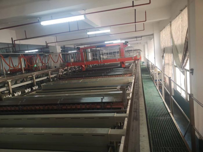
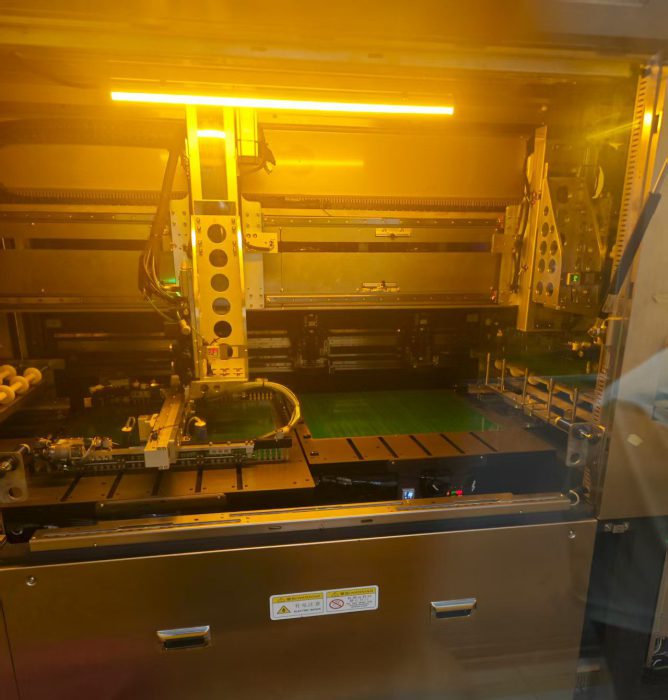
Three Common PCB Copper Plating Process Methods and Their Pros & Cons
In printed circuit board (PCB) manufacturing, copper electroplating is a critical process for building reliable conductive pathways both on the PCB surface and inside plated through-holes (PTH). The choice of plating process directly affects product reliability, manufacturing cost, and delivery time.
This guide explores the fundamentals of copper plating, the three most common PCB copper plating workflows, their step-by-step methods, technical considerations, and pros-and-cons analysis. We will also highlight why SQPCB, with its advanced in-house capabilities, is a trusted partner for global B2B clients seeking quality and delivery control.

PCB Copper Plating Process
Understanding the Basics: Electroless Copper vs. Electrolytic Copper
Electroless Copper (沉铜)
Electroless copper deposition is a chemical process used to deposit an ultra-thin copper layer (typically 0.1–0.3 μm) onto non-conductive surfaces—mainly the walls of drilled holes and the PCB laminate. This creates a conductive seed layer, allowing electrical current to pass during subsequent electrolytic plating.
Electrolytic Copper Plating (电镀铜)
Electrolytic copper plating is an electrical process that uses a plating bath and a direct current to deposit copper onto the seed layer. In PCB manufacturing, copper thickness can be controlled precisely—primary plating (一次铜) typically adds 7–10 μm, while additional plating cycles can achieve the final required copper thickness.
1. Three Common PCB Copper Plating Processes in pcb manufacturing process
1.1 Thick Copper First → Outer Layer Imaging → Copper & Tin Plating → Resist Strip → Etching → Tin Strip
Steps:
Electroless Copper (0.1–0.3 μm) – Deposits the initial conductive layer on hole walls and PCB surfaces.
Full-Panel Electrolytic Copper Plating (Thick Copper) – Adds significant copper thickness across the entire panel, typically to 18–25 μm, ensuring strong base copper and reliable PTH walls.
Outer Layer Dry Film Lamination – Applies a photosensitive resist film.
Exposure & Development – Transfers the circuit image using phototools or LDI (Laser Direct Imaging).
Pattern Copper Plating – Electroplates exposed copper traces to the target finished thickness.
Tin Plating – Electroplates tin onto traces as an etching resist.
Resist Strip – Removes dry film to expose unwanted copper.
Etching – Removes bare copper in non-circuit areas.
Tin Strip – Strips tin to reveal the final copper circuitry.
Best For: Automotive PCBs, power boards, applications needing high copper uniformity.
1.2 Thin Copper → First Copper Plating → Outer Layer Imaging → Second Copper & Tin Plating → Resist Strip → Etching → Tin Strip
Steps:
Electroless Copper (0.1–0.3 μm) – Initial conductive layer.
First Copper Plating (一次铜 7–10 μm) – Adds moderate base copper across the panel.
Outer Layer Dry Film Lamination – Apply photoresist.
Exposure & Development – Define circuit patterns.
Second Copper Plating – Increase copper on traces to finished thickness.
Tin Plating – Protect traces during etching.
Resist Strip – Remove photoresist from non-trace areas.
Etching – Remove unwanted copper.
Tin Strip – Strip tin to complete the circuit.
Best For: High-density interconnect (HDI) boards, telecom boards, designs requiring fine copper thickness control.
1.3 Thin Copper → Thick Copper Plating → Outer Layer Imaging → Etching → Resist Strip
Steps:
Electroless Copper (0.1–0.3 μm) – Initial seed layer.
Full-Panel Thick Copper Plating – Electroplate directly to the required finished copper thickness.
Outer Layer Dry Film Lamination – Apply photoresist.
Exposure & Development – Define circuit traces.
Etching – Remove bare copper without tin plating stage.
Resist Strip – Remove dry film from traces.
Best For: Simple layouts, high-current PCBs, and thick-copper designs where ultra-fine features are not critical.
2. Pros and Cons of Each Process
| Process | Advantages | Disadvantages | Applications |
|---|---|---|---|
| Thick Copper → Pattern Plating → Tin | High PTH reliability, uniform outer copper thickness | More steps, longer cycle, higher copper consumption | Automotive, power electronics |
| Thin Copper → First & Second Copper Plating | Flexible control over copper build-up, suited for fine traces | Requires precise process control, more plating stages | HDI, telecom |
| Thin Copper → Full Thick Copper → Etch | Fewer steps, cost savings (no tin plating/strip) | Not ideal for fine lines, higher side-etch risk | Power boards, simple layouts |
3. Why Choose SQPCB for Copper Plating PCBs
Copper plating is only as good as the equipment and process control behind it. Many PCB failures—like uneven copper thickness, poor solder mask adhesion, or via barrel cracking—can be traced back to insufficient plating quality.
SQPCB stands out by investing heavily in modern inline automation, including:
LDI direct imaging for lines – Eliminates distortion from film-based imaging, ensures fine line accuracy.
LDI direct imaging machine for solder mask – Reduces misalignment, improves solder mask clearance, and enhances appearance.

Automated inkjet legend printing – Avoids operator errors, scratches, and foreign matter contamination.
These investments guarantee high yield, reduced rework, and improved solder mask gloss compared to traditional equipment.
Additionally, SQPCB controls its own lamination, HASL, and ENIG plating lines in-house. This not only ensures consistent quality and stable lead times, but also gives customers greater flexibility in urgent or custom orders. For B2B buyers, having a supplier who controls the full process chain means lower risks, faster turnaround, and predictable quality.
SQPCB’s Advantages in Practice:
By using advanced inline LDI imaging and full in-house plating lines, SQPCB has eliminated traditional risks such as film shrinkage, misregistration, manual handling errors, and uneven copper growth. This ensures that every plated-through-hole and copper trace performs reliably in high-demand applications like automotive electronics, telecom infrastructure, and industrial control systems.
4.The Business Impact of Choosing the Right Plating Process
From a B2B perspective, choosing the right copper plating process (and the right partner) directly impacts:
Reliability: Avoiding hidden defects that could lead to costly recalls.
Cost Efficiency: Reducing scrap and rework through process precision.
Scalability: Supporting both prototype runs and high-volume orders with consistent quality.
Speed: Delivering faster cycle times by cutting unnecessary process steps.
Global OEMs and EMS companies are under constant pressure to reduce costs while maintaining reliability. Partnering with a manufacturer like SQPCB, with advanced equipment and in-house control, gives businesses a competitive edge.
5.Future Trends in PCB Copper Plating
As electronics evolve, copper plating is also advancing:
Pulse Plating Technology: Improves copper distribution in microvias and fine features.
Eco-Friendly Chemistry: Reduces hazardous waste and improves sustainability.
High Aspect Ratio Plating: Supports advanced HDI boards with microvias stacked in multiple layers.
Automation & Data Control: Industry 4.0 smart factories integrate real-time monitoring of plating baths and deposition rates.
SQPCB is already aligned with these trends, leveraging automation and advanced imaging to prepare for next-generation PCB demands.
6. FAQs
Q1: What is the difference between electroless and electrolytic copper plating?
Electroless plating is a chemical process for the initial conductive layer (0.1–0.3 μm). Electrolytic plating uses electric current to build up copper thickness.
Q2: How thick is the first copper plating in PCB manufacturing?
The first copper (一次铜) is typically 7–10 μm, providing a solid base before pattern plating.
Q3: Which process is best for HDI PCBs?
The thin copper → first copper → second copper method offers better copper thickness control for fine-pitch designs.
Q4: Does Shuoqiang perform copper plating in-house?
Yes. Shuoqiang handles all plating stages internally, ensuring quality consistency and faster lead times.
Q5: How does copper thickness affect PCB performance?
Thicker copper improves current capacity and thermal management but increases cost and may limit fine trace capability.
- long board pcb
- Flexible PCBs
- Special PCB
- Express Printed Circuit Board
- Pcb Prototype
- LED PCB
- PCB
- Printed Circuit Board
- Pcb meaning
- Pcb manufacturer
- Rigid pcb board
- Rigid Flex PCB

 Quote
Quote
 E-mail