Printed Circuit Boards (PCBs) are the unsung heroes of modern electronics, serving as the foundational platform for virtually every electronic device we use today. From smartphones to industrial machinery, PCBs provide the necessary connections and pathways for electronic components to communicate and function efficiently. The process of PCB board design is both an art and a science, requiring a deep understanding of electrical engineering, material science, and design principles to create reliable and efficient circuits.
1. Understanding the Basics of PCB board Design
At its core, PCB board design involves creating a layout that allows electrical components to be connected through conductive pathways, signal traces, and other features etched onto a non-conductive substrate. The design process typically includes the following key steps:
a. Schematic Capture: The first step in PCB board design is capturing the circuit’s schematic, which involves creating a diagram that shows how all the components are connected. This schematic serves as a blueprint for the PCB layout.
b. Component Placement: Once the schematic is finalized, the next step is to place the components on the PCB. The placement is critical as it affects the performance, reliability, and manufacturability of the board. Components need to be strategically positioned to minimize signal interference and ensure efficient heat dissipation.
c. Routing: After placing the components, the designer must route the electrical connections between them. This involves creating conductive traces that connect the pins of different components. Proper routing is essential to avoid issues such as signal crosstalk, electromagnetic interference (EMI), and signal integrity problems.
d. Layer Management: Most PCBs have multiple layers to accommodate the complexity of modern electronic circuits. Layer management involves determining how many layers the PCB will have and how the different signals will be distributed across these layers. For instance, power and ground planes are often placed on separate layers to reduce noise and improve performance.
e. Design Rule Check (DRC): Before finalizing the design, a DRC is performed to ensure that all design rules have been followed. This step helps catch any potential errors or violations that could affect the PCB’s functionality or manufacturability.
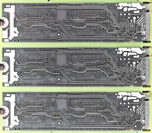
PCB Board Design
2. Key Considerations in PCB board Design
PCB design is not just about connecting components; it’s about optimizing performance, reliability, and cost. Several key considerations play a critical role in achieving a successful design:
a. Signal Integrity: Maintaining signal integrity is crucial, especially in high-speed designs. This involves minimizing noise, reflections, and crosstalk by carefully routing traces, controlling impedance, and using proper termination techniques.
b. Thermal Management: Heat dissipation is a major concern in PCB board design, especially for high-power applications. Proper thermal management techniques, such as using thermal vias, heat sinks, and copper planes, are essential to prevent overheating and ensure the longevity of the components.
c. Power Distribution: Ensuring a stable and reliable power supply to all components is vital. This involves designing power distribution networks (PDNs) with low impedance paths and adequate decoupling capacitors to filter noise.
d. Manufacturability: A well-designed PCB should be easy to manufacture. This means following design guidelines that align with the capabilities of PCB fabrication processes, such as minimum trace widths, via sizes, and spacing between components.
e. Testing and Validation: Once the PCB is designed, it must be tested and validated to ensure it meets all performance and reliability requirements. This includes functional testing, signal integrity analysis, and thermal simulations.
3. The Future of PCB board Design
As technology continues to evolve, PCB board design is becoming increasingly complex. The rise of Internet of Things (IoT) devices, wearable technology, and high-speed communication systems is driving the need for smaller, more powerful, and more efficient PCBs. Designers are now leveraging advanced tools and techniques, such as 3D PCB design, rigid-flex circuits, and high-density interconnect (HDI) technology, to meet these demands.
Additionally, the integration of artificial intelligence (AI) and machine learning (ML) into PCB board design software is revolutionizing the design process. These technologies can optimize component placement, predict potential issues, and even automate parts of the design process, leading to faster development cycles and more reliable designs.
Conclusion
PCB design is a critical aspect of modern electronics, combining engineering principles with creativity to bring innovative electronic products to life. By mastering the art and science of PCB board design, engineers can create circuits that not only meet performance requirements but also contribute to the overall success of electronic devices in a rapidly advancing technological landscape.
our linkedin sqpcb.com

- long board pcb
- Flexible PCBs
- Special PCB
- Express Printed Circuit Board
- Pcb Prototype
- LED PCB
- PCB
- Printed Circuit Board
- Pcb meaning
- Pcb manufacturer
- Rigid pcb board
- Rigid Flex PCB
 Quote
Quote
 E-mail