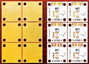
What kind of problem will occur if the PCB thickness is not uniform?
Achieving high-quality printed circuit boards (PCBs) involves precise control over various parameters, from material selection to manufacturing processes. This article delves into critical aspects like resin management, PCB thickness tolerances, and Z0 (characteristic impedance), offering insights for optimizing PCB design and production.

Pcb thickness
1. Vacuum Laminating and Resin Management
A vacuum laminating machine plays a pivotal role in ensuring consistent PCB quality. To enhance performance:
- Reduce the Pressure: Lowering the pressure during the laminating process minimizes glue flow, preserving more resin. Resin content significantly impacts the dielectric constant (εr), which is crucial for electrical performance. A higher resin retention leads to a lower εr, which can improve signal integrity in high-frequency applications.
- Maintain Resin Levels: The dielectric constant is a critical parameter for PCBs, particularly in RF and high-speed digital applications. Preserving more resin ensures a stable and lower εr, optimizing the electrical properties of the board.
2. Controlling Laminate PCB Thickness Tolerances
Uniform laminate thickness is essential for maintaining consistent electrical properties across the PCB. Variations in thickness directly affect the characteristic impedance (Z0) of signal traces:
- Impact on Z0: Non-uniform board thickness leads to variations in the dielectric thickness, causing fluctuations in Z0. Such inconsistencies can degrade signal integrity and result in performance issues, especially in high-frequency applications.
- Tight Tolerances: By adhering to strict thickness tolerances during manufacturing, the reliability and performance of the final product are significantly enhanced.
3. Adhering to Customer-Specified Materials
Meeting customer requirements for PCB material types and specifications is non-negotiable:
- Correct Material Selection: Using the wrong board material or model results in incorrect εr values, compromising Z0 and rendering the board unusable. Strict adherence to material specifications ensures the board meets design criteria.
- Avoiding Errors: Even if the manufacturing process is flawless, deviations in board material type or thickness lead to functional failures, necessitating scrapping of the product.
4. Minimizing Water Absorption
Water absorption can significantly impact the dielectric constant (εr) and, consequently, Z0:
- Avoid Water Absorption: The εr of water is 75, which is drastically higher than most PCB materials. Even slight water absorption can cause a dramatic drop in Z0, introducing instability and affecting performance.
- Protective Measures: Proper storage, handling, and processing techniques can minimize water absorption, preserving the board’s electrical properties.
5. Surface Solder Resistance and Z0 Adjustment
The solder resistance layer on the PCB surface has a measurable impact on Z0 values:
- Impact on Z0: The addition of a solder resistance layer decreases Z0 by 1 to 3Ω. This is due to the higher εr of solder resistance material (εr = 4.0) compared to air (εr = 1).
- Thickness Considerations: Although theoretically, thinner solder resistance layers reduce the impact on Z0, in practice, the effect is minimal and manageable. Still, controlling solder resistance thickness is beneficial for maintaining Z0 within acceptable limits.
6. Inner Layer Line Width and Defect Control
For high-speed and high-frequency applications, controlling inner layer properties is crucial:
- Wire Gaps and Flanges: For signals exceeding 2 GHz, even a 0.05 mm gap can cause unacceptable performance issues, necessitating scrapping of the PCB. Identifying and addressing such defects during the production process is critical.
- Precision in Line Width: Accurate control of inner line width ensures consistent impedance and minimizes signal loss. Defects in the inner layers, such as uneven etching or gaps, must be eliminated to maintain high-performance standards.
7. Key Takeaways for High-Quality PCB Production
Producing high-performance PCBs requires meticulous attention to detail:
- Use vacuum laminating machines effectively to manage resin and minimize glue flow.
- Maintain strict thickness tolerances to ensure uniform dielectric properties.
- Adhere strictly to customer-specified material types and thicknesses.
- Minimize water absorption to preserve stable electrical properties.
- Control solder resistance layer thickness to fine-tune Z0 values.
- Focus on inner layer defect prevention and line width control for high-frequency applications.
By addressing these factors, PCB manufacturers can produce boards that meet the demanding requirements of modern electronic devices. Through precise control and adherence to best practices, manufacturers can deliver reliable, high-performance PCBs that exceed customer expectations.
linkedin https://www.linkedin.com/feed/update/urn:li:activity:
7097167729337532416/
- long board pcb
- Flexible PCBs
- Special PCB
- Express Printed Circuit Board
- Pcb Prototype
- LED PCB
- PCB
- Printed Circuit Board
- Pcb meaning
- Pcb manufacturer
- Rigid pcb board
- Rigid Flex PCB

 Quote
Quote
 E-mail