1. Introduction to Multilayer PCB Stack Up
In the world of modern electronics, devices continue to shrink while becoming more powerful. This relentless trend necessitates more complex interconnections, tighter tolerances, and efficient use of space. The multilayer PCB stack up lies at the heart of this evolution. It serves as the foundational framework that governs signal flow, mechanical integrity, thermal distribution, and electromagnetic compatibility in intricate designs.
A Multilayer PCB consists of more than two copper layers, bonded together with insulating dielectric materials. The configuration is not just a physical arrangement—it’s a functional design that must carefully consider electrical and mechanical constraints. It transforms raw components into coherent, manufacturable systems.
When I first encountered the challenges of designing a stack-up, I underestimated the complexity involved. I believed it was just about choosing a few layers and aligning them. But the reality proved far more intricate. One must consider controlled impedance, EMI shielding, via planning, lamination cycles, and even supplier capability. It’s more than engineering—it’s a multidimensional puzzle.
This complete guide will walk through the principles and nuances of building a robust Multilayer PCB stack up, offering a synthesis of technical knowledge, practical insights, and reflections drawn from real-world projects.
multilayer PCB
2: Historical Evolution of Multilayer PCB Design
Understanding how Multilayer PCB design has evolved provides valuable context. In the early days of electronics, circuits were built using single-sided or double-sided boards. These worked well for radios, televisions, and early computers. But as processing speeds and component densities increased, traditional layouts became insufficient.
The first Multilayer PCBs emerged in the 1960s, primarily in aerospace and military applications. These designs aimed to minimize signal path lengths and offer more complex routing options. By laminating several layers together, engineers achieved higher packaging densities and improved electrical performance.
The introduction of CAD (Computer-Aided Design) tools in the 1980s and 1990s brought a major leap. Stack-up design became more scientific, involving impedance modeling, dielectric simulation, and layer optimization. Surface mount technology (SMT) further fueled the need for multiple layers, especially with the rise of BGA (Ball Grid Array) and HDI (High Density Interconnect) components.
Today, Multilayer PCB stack ups are standard in smartphones, medical devices, servers, EVs, and virtually all advanced electronics. The trend continues toward more layers, thinner dielectrics, and more intricate constructions, such as rigid-flex hybrids and embedded passives.
What fascinates me personally is how this evolution reflects the broader story of electronics: a constant balancing act between space, speed, cost, and reliability. Multilayer PCB stack ups exemplify this balancing act better than perhaps any other element in the electronics industry.
3: Core Principles Behind Multilayer PCB Stack Up
Designing a reliable and high-performance Multilayer PCB stack up requires understanding the fundamental principles that govern how layers interact—both electrically and mechanically. A well-thought-out stack-up structure enhances signal integrity, reduces electromagnetic interference (EMI), manages thermal distribution, and ensures manufacturability.
1. Layer Pairing and Symmetry
One of the core principles in Multilayer PCB stack up design is maintaining symmetry. Each layer in the board contributes to its mechanical stability. Asymmetrical stack-ups can lead to warping during the lamination or reflow soldering process. This is particularly critical when dealing with high-temperature environments or large board formats.
For instance, if you have a power plane close to the top of the stack and nothing to counterbalance it on the bottom, the board may bow or twist. Therefore, designers often pair signal and plane layers symmetrically around the central core or use symmetric dielectric thicknesses to ensure even mechanical stress distribution.
This principle also has aesthetic and intuitive appeal—like balancing a sandwich with equal layers of filling on both sides. It simplifies heat expansion and contraction behavior across the layers.
2. Signal Integrity Through Layer Arrangement
Signal integrity is at the heart of Multilayer PCB design. High-speed signals require specific impedance values to avoid reflections and noise. The arrangement of signal and reference layers (typically power or ground planes) greatly affects this.
A common stack-up configuration involves placing signal layers adjacent to reference planes. This close proximity enables better return current paths, minimizing loop areas and thereby reducing EMI. Designers aim to avoid placing two signal layers next to each other without a reference plane in between, as that invites crosstalk.
3. Dielectric Selection and Control
The dielectric material between copper layers impacts impedance, capacitance, and propagation delay. It also affects thermal conductivity and manufacturability. FR4 remains the standard choice, but higher-performance materials like Rogers, Isola, and Panasonic Megtron are used for RF or high-speed digital designs.
In a Multilayer PCB, uniform dielectric spacing is key for predictable impedance. Designers must define the thickness and dielectric constant (Dk) precisely. The dielectric constant affects how fast a signal travels through the board, which in turn influences timing and synchronization in high-speed designs.
Dielectric selection also impacts the board’s ability to handle temperature and humidity, which in real-world applications can shift signal characteristics over time.
4. Power and Ground Plane Strategy
Another essential principle in Multilayer PCB stack ups is the strategic use of power and ground planes. A solid ground plane serves multiple purposes: providing a return path for signals, enhancing EMI shielding, and stabilizing reference voltages.
Power planes benefit from being placed next to ground planes. The close coupling between these layers forms interplane capacitance, which acts as a decoupling capacitor. This helps maintain clean power delivery to components, especially at high frequencies where discrete capacitors lose effectiveness.
A typical power-ground pair also reduces ground bounce and improves voltage stability across the board, an often overlooked factor in timing-sensitive applications.
5. Impedance Matching and Controlled Trace Geometry
To ensure that signals behave as expected, trace width, spacing, and dielectric thickness must be carefully matched to maintain target impedance. This requires collaboration between layout designers and fabricators, who may use field solvers or impedance calculators to model real-world behavior.
Designers of Multilayer PCB stack ups must specify trace geometry parameters upfront:
-
Microstrip vs. stripline configurations
-
Trace width tolerances
-
Dielectric constant variation
-
Copper thickness considerations
As designs move into the gigahertz realm, even the roughness of copper foil becomes a significant factor in signal degradation and impedance variation.
6. Crosstalk and EMI Mitigation
Minimizing electromagnetic interference and crosstalk is another critical goal. Adjacent signal layers can couple noise if not properly spaced or shielded. Effective stack ups use alternating signal and ground layers to confine electromagnetic fields and reduce interference.
Designers may also:
-
Increase the spacing between high-speed traces
-
Add ground shielding traces (guard traces)
-
Implement stitching vias to maintain ground continuity
-
Route differential pairs closely together on the same layer
In one of my past projects involving a 12-layer CPU carrier board, EMI was a major concern. By rearranging signal layers and inserting more ground planes, we dramatically improved performance without redesigning the whole board.
7. Manufacturability and Layer Count
More layers provide more routing options, but they also increase cost and complexity. The number of layers in a Multilayer PCB must align with design needs and manufacturing capabilities.
Beyond 8–10 layers, issues such as via reliability, lamination cycles, and press-out thickness become critical. Each added layer requires careful attention to registration, drill accuracy, and inner-layer alignment.
This is where communication with PCB fabricators becomes essential. What looks good in CAD may not be practical on the production floor. Stack-up decisions must balance performance aspirations with real-world yield and cost constraints.
4: Materials Selection in Multilayer PCB Stack Up
Material selection is a foundational pillar in the development of a robust and reliable Multilayer PCB stack up. The chosen materials affect every aspect of PCB performance—from electrical behavior and thermal stability to manufacturability and long-term durability. Without thoughtful material decisions, even the most meticulously designed stack-up can fail in real-world conditions.
1. Dielectric Materials: Beyond Just FR-4
The dielectric substrate between conductive layers is one of the most influential materials in a Multilayer PCB stack up. While FR-4 is the industry standard due to its cost-effectiveness and satisfactory performance for general-purpose electronics, it may not suffice for high-speed, high-frequency, or high-reliability applications.
Alternative dielectric materials include:
-
Rogers (e.g., RO4003, RO4350) – These offer low dielectric loss and are suitable for RF and microwave designs.
-
Isola (e.g., IS620, I-Speed) – Ideal for high-speed digital applications and backplanes.
-
Panasonic Megtron – Used in telecom, automotive, and aerospace systems for their low Dk and low loss tangent.
-
Polyimide – Offers excellent thermal stability for aerospace and military-grade applications.
-
Ceramic-filled composites – Employed in extremely high-frequency designs such as radar and millimeter-wave communications.
Each material differs in dielectric constant (Dk), dissipation factor (Df), thermal expansion coefficient (CTE), and glass transition temperature (Tg). These properties impact signal propagation, power integrity, and the board’s ability to survive thermal cycling.
For example, a low Df (loss tangent) is essential in maintaining signal strength across long traces at high frequencies. In one instance, replacing FR-4 with RO4350 allowed a 10Gbps signal to maintain integrity across a 12-inch trace without additional compensation structures.
2. Copper Foils and Their Characteristics
The copper layer in a Multilayer PCB serves as the conductive pathway for signals and power. Copper foils come in different thicknesses and types, depending on performance requirements and manufacturing constraints.
Typical options include:
-
Standard Electrolytic Copper (ED) – Common and cost-effective, but has higher surface roughness.
-
Rolled Annealed Copper (RA) – Smoother surface, ideal for flexible circuits and high-frequency applications.
-
Reverse Treated Copper (RTF) – Provides good adhesion while maintaining moderate smoothness.
-
Very Low Profile (VLP) and Ultra-Low Profile (ULP) – Used in high-speed and high-density PCBs to reduce skin effect and signal loss.
Copper thickness is also a key parameter. Designers usually specify 0.5 oz/ft² (17.5 µm) or 1 oz/ft² (35 µm) copper, but power-intensive applications may use heavier copper (2 oz/ft² or more) to manage current flow and heat dissipation.
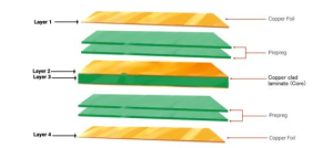
3. Prepregs and Core Laminates
A Multilayer PCB stack up is built using alternating layers of core and prepreg materials. The core is a rigid, cured laminate with copper on both sides, while prepreg is a partially cured glass-reinforced epoxy that bonds adjacent layers during lamination.
The selection and placement of prepreg layers influence:
-
Lamination quality
-
Dielectric thickness control
-
Impedance matching
-
Warpage resistance
High-quality prepregs are essential for achieving uniform dielectric spacing and layer adhesion. Designers must also account for resin flow and glass weave structure, as these can influence etch uniformity and signal skew in high-speed designs.
4. Soldermask and Surface Finish Materials
Though not internal to the stack-up, soldermask and surface finish materials are important complements to Multilayer PCB design. Soldermask prevents oxidation and solder bridging, while surface finishes determine the solderability and shelf life of PCBs.
Common soldermask materials include:
-
LPI (Liquid Photo Imageable) – The most widely used, offering precise coverage and strong adhesion.
-
PSR-4000 series – Widely used in high-reliability automotive and industrial electronics.
Surface finishes include:
-
ENIG (Electroless Nickel Immersion Gold) – Good for fine-pitch components and wire bonding.
-
OSP (Organic Solderability Preservative) – Environmentally friendly and cost-effective.
-
HASL (Hot Air Solder Leveling) – Traditional but less suitable for fine geometries.
-
Immersion Silver or Tin – Useful for high-speed signal integrity due to flat surfaces.
These materials influence overall board thickness, pad planarity, and solder joint reliability. A mismatch in material properties—such as differing CTEs—can result in microcracks, delamination, or solder fatigue.
5. Thermal and Mechanical Considerations
A crucial element in Multilayer PCB material selection is thermal performance. Electronics often operate in elevated temperature environments or endure rapid thermal cycling. Materials must withstand these stresses without cracking or warping.
Important parameters include:
-
Tg (Glass Transition Temperature) – The temperature at which the material softens. Materials with higher Tg are more thermally robust.
-
CTE (Coefficient of Thermal Expansion) – A mismatch between CTEs of copper and dielectric can cause via barrel cracking or delamination.
-
Td (Decomposition Temperature) – Indicates thermal degradation point, especially important for lead-free reflow processes.
Materials like polyimide and high-Tg FR-4 variants help improve survivability in automotive and aerospace environments.
In one product I helped design for a rugged GPS module, switching from standard FR-4 to a high-Tg variant prevented consistent delamination issues during reflow, which ultimately saved thousands in scrap and rework costs.
6. Material Availability and Vendor Support
Finally, designers must consider the availability of materials and their compatibility with the manufacturing process. A material might be ideal on paper but impractical if it’s not readily available, certified, or supported by the chosen fabrication partner.
Close coordination with suppliers is essential, especially for low-volume or prototype runs. For large-scale production, using industry-standard materials with proven reliability and sourcing support can streamline procurement and reduce risks.
5: Electrical Considerations in Multilayer PCB Stack Up
Electrical performance is one of the most critical factors in the design of a Multilayer PCB stack up. As modern electronics continue to operate at higher speeds and with more complex signaling protocols, ensuring that electrical characteristics are well-managed across the board structure becomes essential.
In this section, we’ll explore the core electrical concerns that influence stack-up decisions—including impedance control, signal layer arrangement, power distribution, and noise mitigation. These are the invisible, yet powerful forces shaping whether a circuit will perform reliably in real-world conditions.
1. Characteristic Impedance and Its Importance
One of the central electrical considerations in a Multilayer PCB is the control of characteristic impedance. Impedance mismatches lead to signal reflections, loss of signal integrity, timing issues, and electromagnetic interference (EMI).
In high-speed designs, each trace effectively becomes a transmission line. To ensure predictable performance, the impedance of each trace must match the driver’s output and the receiver’s input.
Typical impedance values include:
-
50Ω for single-ended signals (e.g., clock lines)
-
90Ω or 100Ω for differential pairs (e.g., USB, HDMI, Ethernet)
Impedance is affected by:
-
Trace width and thickness
-
Distance between trace and reference plane
-
Dielectric constant (Dk) of the material
-
Copper roughness and geometry
A key task in stack-up design is setting the dielectric thickness and trace dimensions to achieve target impedance values across all critical nets.
2. Signal Layer Placement and Reference Planes
Signal integrity begins with how signal and plane layers are arranged within the Multilayer PCB stack up. The general rule is to place each signal layer adjacent to a solid reference plane (either ground or power).
This provides the shortest and most stable return path for current, which is especially critical at high frequencies. A poor return path results in wider current loops, which increases susceptibility to EMI and crosstalk.
Designers should avoid placing two signal layers directly next to each other without a reference plane between them. In cases where this is necessary, it becomes vital to increase trace spacing and route critical signals orthogonally to reduce coupling.
3. Power Delivery Network (PDN) Considerations
Delivering clean and stable power to every component is another electrical challenge in Multilayer PCB stack ups. Power and ground planes are not only sources of voltage—they’re also return paths for signal current and sources of electromagnetic energy.
PDN design principles include:
-
Creating wide, low-impedance planes
-
Using closely coupled power and ground layers to form interplane capacitance
-
Placing decoupling capacitors strategically close to IC power pins
-
Minimizing via transitions in power paths
High-speed ICs and FPGAs often demand ultra-low impedance power delivery, with transient responses measured in picoseconds. To meet these demands, designers simulate the PDN using tools such as PI (power integrity) simulators to identify weak points and optimize layer assignments.
4. Crosstalk and Noise Isolation
Crosstalk occurs when a signal on one trace induces noise on a nearby trace. In a Multilayer PCB, improper signal layer planning can make this problem worse. Close routing, improper spacing, or parallel trace runs on adjacent layers all contribute to crosstalk.
Effective countermeasures include:
-
Routing orthogonal signal layers on adjacent levels (e.g., horizontal on L3, vertical on L4)
-
Increasing trace-to-trace spacing (3W rule: width = W, spacing = 3W)
-
Shielding sensitive traces with ground guard traces
-
Using ground reference planes adjacent to signal layers
Another source of noise is ground bounce, caused by simultaneous switching outputs (SSOs) returning through shared ground paths. By maintaining solid ground planes and avoiding split planes under sensitive components, designers can minimize such noise effects.
5. Differential Pair Routing and Layer Considerations
Many modern interfaces (e.g., USB, LVDS, SATA, PCIe) use differential signaling. These pairs require precise impedance control and symmetry throughout the stack up.
Key principles in Multilayer PCB stack up for differential pairs:
-
Route pairs together, maintaining consistent spacing and length
-
Avoid layer transitions unless absolutely necessary
-
Ensure equal dielectric environment around both traces
-
Place the pair adjacent to a solid reference plane for clean return currents
In my experience, one overlooked issue is via placement along the pair. Unequal via counts or poorly matched paths can degrade signal integrity, especially as frequencies increase. Controlled layer transitions with back-drilled vias or via-in-pad techniques are often used in high-speed boards.
6. Managing Skew, Delay, and Propagation Time
As trace lengths grow and signal rise times shrink, timing mismatches become more significant. This is especially true in parallel bus systems or multi-gigabit serial links.
Electrical design within a Multilayer PCB stack up must account for:
-
Skew (difference in arrival times between signals)
-
Propagation delay (typically measured in ps/inch)
-
Matched lengths for differential or parallel buses
Skew can be reduced by tuning trace lengths and using consistent dielectric materials across matched nets. Designers also route critical nets on inner layers to shield them from external noise and maintain tighter impedance control.
7. Managing High-Speed Signals and Losses
In high-speed designs (e.g., >2GHz), signal losses due to dielectric absorption, copper surface roughness, and radiation become major challenges. Multilayer PCB stack ups must be optimized to reduce these losses by:
-
Choosing low-loss dielectric materials (e.g., Rogers, Megtron, Nelco)
-
Using smooth copper foils (e.g., VLP, HVLP)
-
Shortening signal paths
-
Using wider traces or stripline configurations
In a recent 10G Ethernet design, switching from standard FR-4 to a low-loss laminate reduced insertion loss by over 40%, enabling error-free transmission at the required link margin.
Conclusion and Best Practices Summary for Multilayer PCB Stack Up
Multilayer PCBs are essential for advanced electronics, offering high performance and miniaturization. Proper design and manufacturing techniques are crucial for reliability.
Designing a reliable, manufacturable, and high-performance Multilayer PCB stack up is a multifaceted challenge. It demands careful consideration of electrical, thermal, mechanical, and cost factors, while embracing emerging technologies and collaborating closely with fabricators.
Throughout this guide, we have explored the fundamental principles and advanced techniques that empower engineers to build stack ups that not only meet—but often exceed—design objectives. Here, we distill these insights into a clear set of best practices to carry forward into every multilayer PCB project.

- long board pcb
- Flexible PCBs
- Special PCB
- Express Printed Circuit Board
- Pcb Prototype
- LED PCB
- PCB
- Printed Circuit Board
- Pcb meaning
- Pcb manufacturer
- Rigid pcb board
- Rigid Flex PCB
 Quote
Quote
 E-mail