Introduction to LPI Solder Mask in PCB Manufacturing
The LPI (Liquid Photoimageable) solder mask in PCB manufacturing is an essential part of modern PCB manufacturing, primarily serving to protect copper traces from oxidation, prevent solder bridging, and ensure the mechanical and chemical integrity of the final board. With the continual miniaturization of electronic components and increased design complexity, the role of the LPI solder mask has evolved from a protective coating into a critical enabler of high-density, high-reliability circuit boards.
Historically, screen printing was widely used for applying solder mask, but it lacked precision and repeatability. The LPI process changed that. By enabling fine-resolution patterning, it became the industry standard for most high-performance PCBs. The adoption of LPI solder mask represents not just a process improvement but a shift in manufacturing philosophy—from bulk application to precision-engineered surface management.
The evolution of printed circuit board (PCB) manufacturing has continuously demanded higher precision, reliability, and durability in protective coatings. Among these, the LPI Solder Mask, or Liquid Photoimageable Solder Mask, has emerged as one of the most widely adopted technologies in the industry. As electronics continue to shrink and functionality increases, manufacturers have had to pivot to solutions that offer fine-line resolution, better dielectric properties, and long-term environmental protection.
This article delves into the complete landscape of LPI Solder Mask in PCB manufacturing. It begins by establishing the historical context and rationale behind the development of solder masks and then transitions into the specific advantages and implementation considerations of LPI technologies. Throughout this piece, I will integrate my personal thoughts and observations, highlighting not only the technical intricacies but also the broader implications on manufacturing trends, cost efficiency, and environmental impact.
Importantly, while the term LPI Solder Mask in PCB manufacturing will be used as required in subheadings and analysis, it will be employed with moderation in the main body to avoid unnecessary repetition and maintain readability.
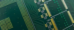
LPI Solder Mask
2. The Role of LPI Solder Mask in PCB Fabrication
In any PCB, copper traces form the conductive pathways for electronic signals. However, these traces are susceptible to environmental degradation. The LPI solder mask in PCB manufacturing plays a preventive role by covering the non-soldered areas, thereby limiting exposure to air, moisture, and other corrosive agents. But its function goes beyond protection.
During soldering, molten solder can easily create shorts between adjacent pads if not properly isolated. The LPI solder mask in PCB manufacturing acts as a physical barrier, preventing such shorts, especially in dense BGA (Ball Grid Array) or QFN (Quad Flat No-lead) packages. Its role becomes critical in multi-layer boards where alignment accuracy is vital. Moreover, modern assembly lines require consistency, and the photoimageable nature of LPI solder masks ensures precise and repeatable application.
In my experience working with fabrication teams, the shift from traditional epoxy or thermal cure masks to LPI systems directly correlates with improved yield and reduced post-assembly rework. The decision to use LPI solder mask is not merely technical—it is also economic.
3. Chemical Composition and Properties of LPI Solder Mask
The chemical formulation of LPI solder mask includes photo-initiators, resins (often epoxy-based), and various solvents. These materials are chosen for their UV sensitivity, mechanical strength, thermal resistance, and chemical stability. After application and development, the mask must remain stable during reflow soldering processes where temperatures can exceed 240°C.
An ideal LPI solder mask will have the following characteristics:
-
High adhesion to copper and laminate
-
Resistance to flux and cleaning chemicals
-
Excellent thermal endurance
-
High dielectric strength
-
Fine resolution capability
However, these ideal properties must be balanced. For example, increasing solvent resistance can make the development process more challenging. Thus, LPI solder mask chemistry is often tailored to specific process requirements. Some PCB manufacturers even work directly with material suppliers to customize formulations for ultra-HD circuit boards.
From a broader perspective, this customization indicates a trend toward vertical integration in the PCB supply chain—where LPI solder mask technology becomes a strategic differentiator.
4. LPI Solder Mask Application Process in PCB Manufacturing
The LPI solder mask application process involves several steps, each critical to the final performance of the PCB. Here is an outline of the standard flow:
-
Surface Cleaning: The bare PCB is cleaned using mechanical or chemical methods to ensure optimal mask adhesion.
-
Coating: The LPI mask is applied via curtain coating, spray coating, or screen printing.
-
Pre-Drying: A tack-dry step solidifies the coating slightly to enable image exposure without flow.
-
Exposure: UV light is used to transfer the solder mask pattern from a photo-tool.
-
Development: Unexposed areas are washed away using an alkaline solution.
-
Final Cure: A thermal or UV cure step hardens the mask into its final state.
Each of these stages requires precise control. Any contamination, misalignment, or deviation in cure profile can lead to failure modes such as poor adhesion, solder bridging, or even complete delamination during reflow.
In my view, one of the most underestimated stages is pre-drying. Many failures attributed to poor exposure or development can be traced back to improper solvent removal before UV curing. As such, line engineers must constantly monitor humidity, oven temperatures, and material viscosity to ensure consistency.
5. Key Advantages of Using LPI Solder Mask in PCB Manufacturing
The preference for LPI solder mask over alternative solder mask types is driven by a variety of advantages:
-
High Resolution: Enables fine-pitch designs necessary for modern microelectronics.
-
Cost Efficiency: Lower defect rates reduce rework costs.
-
Consistency: Automated exposure and development provide uniform results.
-
Durability: Enhanced chemical and thermal resistance in harsh operating conditions.
-
Environmental Control: Compared to older technologies, modern LPI masks have lower VOC emissions and reduced material waste.
For high-reliability sectors like aerospace, automotive, and medical electronics, these advantages are not optional—they are prerequisites. I’ve seen how even a small improvement in solder mask alignment or adhesion can impact the MTBF (mean time between failure) of mission-critical products.
In some of the newer designs involving flexible-rigid hybrids, the ability of LPI solder mask to conform to intricate surface topographies is especially important. Its flow behavior can be controlled by viscosity adjustments, allowing precise coating without overburdening sensitive areas.
6. Limitations and Challenges of LPI Solder Mask in PCB Manufacturing
Despite its advantages, the use of LPI solder mask in PCB manufacturing is not without limitations. Understanding these challenges is essential for both design engineers and process managers.
One primary concern is exposure sensitivity. Because the patterning relies on UV light, even slight misalignment or exposure variability can lead to underdeveloped or overdeveloped features. For extremely fine-pitch designs, this is a significant challenge, especially when the mask opening must align with solder pads smaller than 100 microns.
Another limitation involves surface topography. While LPI solder mask can adapt to modest surface variations, it may struggle to provide consistent coverage on highly irregular surfaces, such as boards with heavy copper or uneven via filling. Insufficient coverage may result in “tenting failures,” where vias are only partially sealed, leading to potential contamination.
Thermal expansion mismatch between the solder mask and substrate can also create delamination risks during repeated thermal cycling, particularly in automotive or aerospace environments.
In my observation, another underrated challenge is developer chemistry control. Over time, the developer solution can become saturated, reducing the effectiveness of unexposed mask removal. This is a hidden cause of poor solder mask definition that many new facilities fail to anticipate.
Recognizing these challenges allows for better process engineering and risk mitigation strategies in high-volume PCB production.
7. LPI Solder Mask in High-Density PCB Manufacturing
As electronic devices continue to shrink while offering increased functionality, high-density interconnect (HDI) designs have become the norm. These designs place stringent demands on all PCB manufacturing steps, especially the application of the LPI solder mask.
In HDI boards, the pad pitch may be below 0.5 mm, requiring extremely precise solder mask alignment. Here, the photoimageable nature of LPI solder mask truly shines. The mask can be patterned with sub-50-micron accuracy, enabling clean separation between adjacent pads—even in BGA and CSP (Chip Scale Package) layouts.
Furthermore, the ability to use “solder mask defined pads” (SMD) allows designers to increase component density without sacrificing reliability. This technique involves intentionally shrinking the mask opening to reduce the exposed pad area, helping to control solder joint geometry and reduce the risk of bridging.
However, this approach places extra emphasis on mask registration and dimensional stability. Any misalignment during exposure or cure will compromise pad definition and lead to assembly defects.
I’ve found that in HDI designs, collaboration between the layout engineer and the fabrication team is essential. Decisions about solder mask design rules should not be made in isolation. By accounting for the limitations and capabilities of LPI solder mask technology early in the design cycle, better yield and board performance can be achieved.
8. Environmental Considerations for LPI Solder Mask in PCB Manufacturing
As sustainability becomes increasingly important across the electronics industry, the environmental aspects of LPI solder mask usage warrant attention. While it’s more eco-friendly than some legacy materials, LPI solder mask still involves solvents, developers, and curing emissions that require proper management.
Modern formulations have reduced volatile organic compound (VOC) content and are often RoHS-compliant, meaning they avoid restricted substances like lead, mercury, or hexavalent chromium. However, the application and development processes still produce waste streams, especially alkaline developer runoff, that must be treated before disposal.
Energy consumption is another factor. The UV exposure systems, clean rooms, and baking ovens involved in applying LPI solder mask add to the carbon footprint of PCB production. That said, the process is significantly cleaner and more efficient than older alternatives like thermal-cured epoxy masks.
From a personal standpoint, I believe environmental stewardship in PCB manufacturing isn’t just about regulatory compliance—it’s a competitive advantage. Manufacturers who adopt low-emission solder mask materials and closed-loop processing systems will be better positioned as environmental policies become stricter.
9. Quality Control Procedures for LPI Solder Mask in PCB Manufacturing
Ensuring the consistent quality of LPI solder mask application is vital to final board performance. Quality control (QC) procedures focus on both visual and functional attributes, from initial coating thickness to final adhesion.
Some standard QC tests include:
-
Cross-section analysis to inspect coating thickness and adhesion
-
Tape pull tests to verify adhesion strength after curing
-
Solderability testing to ensure mask does not interfere with soldering
-
AOI (Automated Optical Inspection) to detect pattern defects like underdeveloped mask or misaligned openings
-
Solvent resistance checks to confirm chemical durability
Additionally, registration accuracy is measured using fiducial alignment markers during exposure and verified through microscope inspection.
Process parameters such as UV intensity, bake temperature, and developer concentration must also be closely monitored and recorded. Statistical process control (SPC) charts are commonly used in advanced fabrication lines to detect trends and correct drift before defects occur.
In my professional practice, one lesson I’ve learned is that early process feedback is critical. Catching mask-related issues before reflow or assembly stages dramatically reduces repair costs and customer complaints.
10. Comparative Analysis: LPI Solder Mask vs. Other Masking Methods in PCB Manufacturing
When comparing LPI solder mask with other solder mask types—such as dry film or thermal cure epoxies—its superiority becomes apparent in terms of resolution, process flexibility, and environmental profile. However, each method has its niche, and the decision depends on application specifics.
| Feature | LPI Solder Mask | Dry Film Mask | Thermal Cure Epoxy |
|---|---|---|---|
| Resolution | High (down to ~50 µm) | Medium | Low |
| Conformality | Excellent | Poor on irregular surfaces | Good |
| Cost Efficiency | Moderate | High | Low |
| Environmental Profile | Moderate (RoHS/low VOC) | Poor (older methods) | Variable |
| Automation Compatibility | High | Low | Moderate |
Dry film masks are often used when mechanical strength is paramount, such as in high-voltage boards, but their inability to conform to irregular surfaces limits their use. Thermal cure epoxies are durable and inexpensive but lack the fine detail achievable with LPI solder mask.
In conclusion, LPI solder mask offers the best balance of precision, performance, and practicality for most modern PCB applications. Its compatibility with automation also makes it suitable for high-volume manufacturing.
11. Role of LPI Solder Mask in PCB Reliability and Longevity
One of the most vital contributions of LPI solder mask in PCB manufacturing is its effect on the long-term reliability of the finished product. In harsh environments—such as those found in automotive, aerospace, and industrial applications—the solder mask must provide both chemical protection and mechanical reinforcement.
LPI solder mask helps prevent oxidation of exposed copper, blocks moisture ingress, and serves as a barrier against ionic contaminants that could lead to dendritic growth or electrical leakage. Additionally, it minimizes mechanical stress on solder joints by absorbing some of the thermal expansion and contraction that occurs during power cycles.
In multilayer boards, especially those with HDI structures or embedded components, the durability of the solder mask becomes critical. Delamination or cracking of the mask can expose inner layers, leading to latent failures. LPI formulations with high Tg (glass transition temperature) and robust adhesion properties help maintain board integrity even under thermal shock or vibration.
From my experience, many field failures attributed to “intermittent shorts” or “cold solder joints” often trace back to poor solder mask coverage or degradation. Thus, investing in a high-quality LPI solder mask and ensuring its proper application is a proactive measure in product assurance—not just a manufacturing requirement.
12. Automation and Robotics in Applying LPI Solder Mask in PCB Manufacturing
As PCB manufacturing scales up to meet global demand, automation has become indispensable. LPI solder mask application is particularly well-suited to robotic and CNC-based systems, which improve precision, consistency, and throughput.
Automation is commonly employed in the following areas:
-
Coating equipment: Curtain coaters and spray coaters are robotically controlled to apply uniform layers of LPI solder mask, regardless of panel size or design complexity.
-
Exposure systems: Direct imaging systems using laser or LED projectors eliminate the need for photo-tools and allow faster changeovers.
-
Developer and cure ovens: Automated handling lines ensure consistent timing, temperature, and chemical exposure during development and curing.
The integration of machine vision systems with exposure tools also improves registration accuracy. Alignment is verified in real-time, reducing the risk of mask misplacement on fine-pitch designs.
My personal observation is that automated LPI solder mask application has become a strategic advantage. Companies that invest in advanced robotic systems not only reduce operational errors but also enhance their ability to deliver consistently high-quality boards to demanding markets such as medical devices and aerospace.
13. Cost Implications of Using LPI Solder Mask in PCB Manufacturing
While the LPI solder mask is often more expensive per liter than traditional materials, the total cost of ownership tells a different story. When evaluating the economics, one must consider direct costs (materials, labor, energy) and indirect costs (yield loss, rework, field failures).
Here are some cost-related advantages:
-
Lower rework rates: Fewer solder bridges or pad contamination issues.
-
Higher process yields: Better registration and finer features reduce scrap.
-
Reduced photo-tooling needs: With digital exposure systems, tooling costs are eliminated.
-
Scalability: Suitable for both prototyping and mass production, minimizing transition costs.
However, it is essential to balance the upfront investment in equipment (e.g., direct imaging machines) and infrastructure (clean rooms, controlled ovens) with the long-term savings. In many cases, smaller manufacturers may initially resist the switch due to capital constraints.
In my view, any PCB manufacturer planning for long-term competitiveness should embrace LPI solder mask as a baseline capability. The initial costs are quickly offset by gains in consistency, speed, and market acceptance.
14. Innovations and Future Trends of LPI Solder Mask in PCB Manufacturing
As the PCB industry continues to evolve, innovations in LPI solder mask technology are keeping pace. Several key trends are shaping the next generation of solder mask materials and processes.
-
Ultra-thin masks: To meet the needs of 01005 component packages and sub-0.3mm pitch BGAs, new formulations offer thinner coverage while retaining dielectric strength.
-
High-frequency compatibility: For RF and microwave PCBs, newer LPI solder masks are engineered to minimize signal loss at GHz frequencies.
-
Low-temperature curing: Advanced chemistries enable full cure at lower temperatures, ideal for flexible substrates or mixed-material assemblies.
-
Antimicrobial solder masks: For medical electronics, masks infused with antimicrobial agents help reduce surface contamination.
Additionally, AI-driven process control is being introduced to fine-tune coating thickness, exposure energy, and cure profiles in real time. Machine learning models can detect trends leading to solder mask defects before they happen, further reducing downtime and material waste.
I believe the convergence of materials science, AI, and digital imaging will eventually produce self-adapting LPI solder mask systems—coatings that sense and correct their own alignment or thickness in response to design features. This vision may not be far off, especially as Industry 4.0 principles take deeper root in the electronics supply chain.
15. Conclusion and Future Outlook on LPI Solder Mask in PCB Manufacturing
The journey of LPI Solder Mask in PCB manufacturing reflects not only technological advancement but also the evolving priorities of the electronics industry—where miniaturization, reliability, compliance, and sustainability are more critical than ever.
Throughout this article, we have examined LPI solder mask from every angle: from its chemistry and application methods, to process control, defect prevention, inspection, environmental responsibility, cost analysis, and real-world applications. Now, as we conclude, it’s clear that LPI solder mask has become much more than a passive protective coating—it’s a strategic enabler of modern electronic design and manufacturing.
In my own experience, I’ve witnessed how LPI Solder Mask in PCB manufacturing has evolved from a quality assurance afterthought to a precision-driven, value-added process. Manufacturers who treat the solder mask process with the same rigor as copper etching or drilling often experience better yields, fewer customer returns, and faster development cycles.
Moreover, I believe LPI solder mask will be an important touchpoint in future electronic ecosystems—where substrates, coatings, and embedded intelligence blend into a seamless, multifunctional platform. As demands increase for wearable, foldable, and mission-critical electronics, LPI’s role will only grow more vital.
The future of LPI Solder Mask in PCB manufacturing is not just about better protection—it’s about enabling the next generation of electronics to be smarter, cleaner, smaller, and more reliable. As both designers and manufacturers push boundaries, LPI solder mask technology stands ready to evolve alongside them.

- long board pcb
- Flexible PCBs
- Special PCB
- Express Printed Circuit Board
- Pcb Prototype
- LED PCB
- PCB
- Printed Circuit Board
- Pcb meaning
- Pcb manufacturer
- Rigid pcb board
- Rigid Flex PCB
 Quote
Quote
 E-mail