Understanding Light Bare Boards in PCB Manufacturing
Introduction
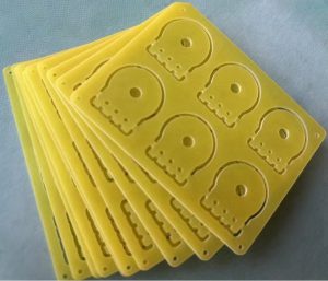
The foundation of any electronic device lies in its Printed Circuit Board (PCB). A bare board refers to a PCB that lacks populated components but has undergone the initial steps of manufacturing—copper cladding, etching, and drilling. The image you provided shows an example of a light bare board—a specially designed PCB used primarily in prototyping, small production runs, or specific design testing. Unlike standard bare boards, light boards are often used in situations where precision design is critical and component placement plays an important role, as indicated by their pre-etched patterns.
This article explores the unique features, manufacturing process, and applications of light bare boards, focusing on their role in rapid prototyping, product testing, and low-volume production.
Light Bare Board
What is a Light Bare Board?
A light bare board (sometimes called a prototype board or pre-production PCB) is a type of unpopulated PCB designed for use in testing and prototyping. It is characterized by pre-defined holes, etched outlines, and sometimes custom patterns for component placement. Light bare boards are typically created when engineers and manufacturers want to evaluate a circuit design before committing to mass production.
For instance, the board in the image you provided shows pre-etched patterns of shapes—such as skulls—designed into the PCB, which is often used to test or validate a particular design. These designs help in the testing of various component placement techniques and assembly methods that will later be used on the final product.
Key Characteristics of Light Bare Boards
- Unpopulated: Light bare boards do not have components mounted on them yet. They only consist of substrate material (usually FR4 or other flexible materials) and etched copper traces, which form the electrical pathways between components.
- Pre-etched Patterns: Unlike standard bare boards, light boards often come with pre-etched patterns such as the skull design shown in the image. These patterns serve a variety of purposes—such as component alignment or test patterns.
- Pre-drilled Holes: The light bare boards usually feature pre-drilled holes in the correct locations for component leads or for connecting different layers of a PCB (if the board is multi-layered). These holes may be for vias (electrical interconnections between layers) or for mounting components like connectors, resistors, or capacitors.
- Customization: Light bare boards are often customized based on specific design requirements, making them ideal for low-volume production or prototype testing.
Manufacturing Process of Light Bare Boards
The manufacturing process of light bare boards follows a similar path to traditional PCB manufacturing, but with specific attention to the requirements for prototypes or testing. Here’s an overview of the steps:
1. Design and Schematic Creation
The first step is to create the circuit design using Electronic Design Automation (EDA) software. Engineers will define the copper traces, via placement, and component pads. For light bare boards, the design may include test patterns or component shapes that are important for the specific application or testing process. Once the design is finalized, it is converted into Gerber files—the industry standard format for PCB manufacturing.
2. Substrate Material Selection
The substrate is chosen based on the intended application of the light bare board. Common materials include FR4 (fiberglass-based epoxy) or polyimide (for flexible PCBs). The substrate provides the mechanical strength for the bare board and supports the copper traces.
3. Copper Cladding
After selecting the substrate, a thin layer of copper foil is laminated onto the surface of the board. The copper layer forms the electrical pathways, allowing the board to function as an electronic circuit once the components are added. For light bare boards, the copper cladding is crucial for conducting electricity between the components in later stages of assembly.
4. Photolithography and Etching
Once the copper cladding is applied, photolithography is used to transfer the design onto the board. The photoresist material is applied to the copper surface and exposed to ultraviolet (UV) light through a mask that contains the design pattern. The areas exposed to the UV light harden, and the unexposed areas are washed away.
The board is then etched using a chemical solution, removing the unwanted copper and leaving only the traces that form the circuit pathways. This is where the skull patterns or other test patterns are created. These patterns serve as the layout for testing or as visual cues for later stages of production.
5. Drilling the Holes
For light bare boards, precise drilling is crucial to ensure that the holes align perfectly with the copper traces and components. Drill holes are created for vias (connections between layers) and for mounting components. These holes are usually drilled with high-precision equipment to avoid misalignment.
6. Surface Finish and Inspection
Once the holes are drilled, the board is plated with a thin layer of metal (such as gold, tin, or silver) to prevent oxidation and to improve solderability for component placement. The board undergoes rigorous inspection using tools like Automated Optical Inspection (AOI) to check for defects such as misaligned holes, improper etching, or unwanted copper traces.
Applications of Light Bare Boards
Light bare boards are particularly useful in applications where flexibility, rapid prototyping, and testing are crucial. Some of the common applications include:
1. Prototyping and Product Development
Light bare boards are often used in the initial stages of product development for prototyping. Engineers can create custom designs, place components, and test the functionality of a circuit before committing to full-scale production. By using light bare boards, they can identify potential issues early in the development process and make adjustments as needed.
2. Testing and Validation
Before moving forward with mass production, manufacturers often use light bare boards for testing and validation purposes. These boards allow for the testing of component placement, circuit design, and the board’s overall performance under various conditions.
3. Low-Volume Manufacturing
For companies that need small quantities of a specific design, light bare boards are ideal. These boards are particularly beneficial when mass production is not required, allowing companies to produce limited batches of a product with specialized components or features.
4. Educational and DIY Projects
In educational settings and DIY electronics projects, light bare boards are often used to allow students or hobbyists to practice soldering and circuit building without the complexity of a fully populated PCB.
Conclusion
Light bare boards play a crucial role in the development and manufacturing of Printed Circuit Boards (PCBs). Serving as the unpopulated, initial stage of a PCB, they are essential for prototyping, testing, and low-volume production. Their unique features, such as pre-etched patterns, drilled holes, and copper traces, make them ideal for a variety of applications in both commercial and educational settings.
With the increasing need for rapid prototyping and more flexible production processes, light bare boards offer a cost-effective solution for creating high-quality, functional PCBs for numerous industries, including consumer electronics, automotive, medical devices, and more. Understanding their significance in the PCB manufacturing process helps ensure that the final product is both reliable and efficient.

- long board pcb
- Flexible PCBs
- Special PCB
- Express Printed Circuit Board
- Pcb Prototype
- LED PCB
- PCB
- Printed Circuit Board
- Pcb meaning
- Pcb manufacturer
- Rigid pcb board
- Rigid Flex PCB
 Quote
Quote
 E-mail