LDI exposurer: In the ever-evolving world of PCB manufacturing, precision and consistency aren’t just desirable—they’re non-negotiable. As circuit designs grow more complex and line widths continue to shrink, traditional phototooling methods have begun to show their limits. This is where LDI exposurer—short for Laser Direct Imaging exposure—steps in as a game-changer.
But here’s the kicker: LDI exposurer isn’t just another upgrade. It’s a necessary leap forward if you want to stay competitive, improve yields, and meet the ever-stringent demands of IPC Class 3 manufacturing.
Let’s explore the working principle, evolution, types, benefits, and why LDI exposurer has become an indispensable part of modern PCB manufacturer.
1. What is LDI Exposurer?
LDI exposurer refers to the use of a laser system to directly expose photoresist-coated PCB panels without the need for traditional film phototools. Unlike old-school exposure machines that rely on physical masks, LDI systems project digital patterns generated from the Gerber file directly onto the board surface.
This process significantly enhances accuracy, alignment, and production flexibility.
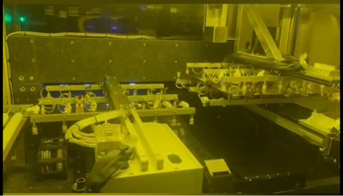
LDI exposurer
2. How LDI Works: The Principle Behind the Technology
At its core, the LDI system uses ultraviolet laser diodes to selectively expose areas of photoresist on the PCB. Here’s how it unfolds:
- The board is coated with a light-sensitive resist.
- A digital pattern (based on your CAD/Gerber data) is fed into the LDI system.
- Precision-controlled laser beams scan across the resist layer to “draw” the circuit pattern.
- The exposed areas are then developed, revealing the pattern for etching or plating.
No films, no alignment headaches, no shrinkage or distortion. Just ultra-clean, accurate imaging.
3. LDI Exposurer for Trace Imaging vs. Solder Mask
LDI exposurer is not limited to just circuit traces. It now plays a crucial role in solder mask imaging as well.
- Trace Imaging (线路曝光): Used for defining copper traces. Accuracy is critical here, especially for HDI and sub-75μm lines.
- Solder Mask Imaging (阻焊曝光): Critical for BGA pads, fine-pitch components, and ensuring mask dam integrity.
At SQPCB, we’ve adopted both LDI trace exposurer and LDI solder mask exposurer machines to ensure high-definition circuit imaging and superior solder mask registration—critical for IPC-6012 Class 3 compliance.
4. The Evolution of LDI Exposurer: From Film to Fully Digital
Let’s rewind a bit.
- Before 2000s: Film phototools were the industry standard. Manual alignment, wear-and-tear, and dimensional instability were ongoing issues.
- Early 2000s: First-generation LDI systems emerged—expensive, slow, and primarily used by high-end fab houses.
- 2010s: Second-generation machines brought cost reductions, faster throughput, and better automation.
- Today: Third-generation LDI exposurer systems feature dual-table designs, inline automation, dynamic focus control, and sub-20μm registration accuracy.
The evolution has been nothing short of transformative.
5. Why LDI Is Now a Necessity, Not a Luxury
Here’s where it gets interesting…
If your PCB shop is still using film-based exposures, you’re already behind. Why? Because:
- Miniaturization: Sub-75μm traces are now common.
- Quick Turns: Digital imaging eliminates time spent on film prep and registration. important machines for express PCB
- Yield: Better alignment = fewer defects = higher production yield.
- Environmental Impact: No films, chemicals, or waste from imaging masks.
That’s why many advanced PCB manufacturers like SQPCB have heavily invested in LDI exposurer. As SQPCB engineers put it, “LDI isn’t just faster—it’s smarter. It’s what enables our factory to deliver high-mix, high-reliability PCBs at speed.”
6. Types of LDI Exposurer Equipment
Not all LDI systems are built the same. Depending on your production size and precision requirements, here are the main types:
| LDI Type | Description | Best Use Cases |
|---|---|---|
| Single Table | One exposure station; lower throughput | Prototyping, small batch |
| Dual Table | Two stations; one loads/unloads while other exposes | Medium-to-high volume, improves productivity |
| Inline (联线) | Fully automated; integrates developer, loader, unloader | High-volume, HDI boards, smart factories |
SQPCB employs dual-table LDI exposurer systems to ensure efficient, high-precision exposure for both standard and advanced PCBs.
7. LDI Machine Price: Is It Worth the Investment?
Short answer: Yes, if you value yield and time.
- Entry-Level LDI (Single Table): $180,000–$250,000
- Dual Table Mid-range: $300,000–$450,000
- Inline Fully Automated: $600,000–$1M+
While this may seem costly, consider the ROI:
- No phototools to maintain
- Reduced defect rate and rework
- Shorter time-to-market
- Perfect registration on every panel
For PCB suppliers targeting high-reliability markets—automotive, aerospace, telecom—this is a no-brainer.
8. Key Benefits of Using LDI Exposurer
Let’s break it down into specifics:
| Benefit | Description |
|---|---|
| Precision Alignment | Digital accuracy ensures repeatability and registration within ±10μm |
| High Throughput | Dual/inline systems process multiple panels per minute |
| Lower Costs Over Time | No film, lower reject rates, less rework |
| Environmental Advantage | Fewer chemicals, less waste |
| Design Flexibility | Easy to switch patterns, no tooling delays |
9. Who Should Use LDI Exposurer?
LDI exposurer is ideal for:
- High-density interconnect (HDI) PCB fabrication
- IC substrates and semiconductor packaging
- Automotive and aerospace circuit boards
- Medical and telecom boards with tight tolerances
- Prototyping houses offering quick-turn capabilities
If your products involve 3mil line/space or Class 3 requirements, LDI is not optional—it’s mandatory.
10. SQPCB: A Leader in LDI Innovation
At SQPCB, we’ve fully integrated LDI exposurer systems for both trace and solder mask imaging.
This gives us the ability to:
- Produce ultra-fine line widths with superb edge definition
- Achieve solder mask precision that surpasses conventional standards
- Shorten lead times by eliminating phototool setup
- Deliver higher yield, especially for multilayer and HDI boards
If you’re seeking a partner that pairs high-end equipment with skilled engineers, SQPCB has the solution.
Conclusion: The Future Is LDI
As circuit density increases and lead times shrink, LDI exposurer stands at the intersection of speed, precision, and cost-effectiveness. It’s the only imaging method that meets modern demands without compromise.
Whether you’re building next-gen IoT devices, automotive ECUs, or aerospace controls, LDI offers the imaging accuracy your project can’t afford to live without.
Partner with innovators. Partner with SQPCB—where precision meets performance.
FAQ Section
Q1: What does LDI exposurer stand for in PCB manufacturing?
A: LDI exposurer stands for Laser Direct Imaging, a cutting-edge process used to expose photoresist directly on the PCB using high-precision laser beams instead of traditional film-based phototools. It transforms Gerber data into a digital pattern, which is then projected onto the board’s surface. This eliminates film distortion, shortens production time, and significantly improves alignment accuracy—especially for fine-line and HDI designs.
Q2: How is LDI exposurer different from traditional phototooling?
A: Traditional phototooling requires physical films (also called photomasks), which are manually aligned and exposed using UV light. This process is prone to distortion, misalignment, and film wear over time. In contrast, LDI exposurer uses a fully digital method where the circuit pattern is imaged directly onto the resist layer via laser beams. This not only improves precision (within ±10μm) but also enhances repeatability and allows for faster job changes without making or replacing film sets.
Q3: What are the advantages of using LDI exposurer for solder mask layers?
A: LDI exposurer delivers superior accuracy and tighter registration for solder mask openings, especially around high-density BGA and fine-pitch components. It helps reduce defects like solder bridging, short circuits, and misalignment during assembly. Unlike traditional screen printing or film methods, LDI allows for dynamic adjustments and on-the-fly corrections to the pattern, ensuring higher yields and improved IPC Class 3 compliance.
Q4: Is LDI exposurer suitable for prototyping and low-volume PCB manufacturing?
A: Absolutely. LDI technology is well-suited for quick-turn prototyping and low- to mid-volume runs due to its film-less, agile nature. Single-table or small-footprint LDI systems enable fast job changes, minimal setup, and no need for costly tooling. Engineers can iterate designs more quickly while maintaining high imaging accuracy, which is crucial when time-to-market and design flexibility are top priorities.
Q5: What is the typical resolution or accuracy of modern LDI exposurer systems?
A: Most industrial-grade LDI exposurer machines offer resolutions of 25μm or better, which supports 3mil/3mil line/space patterns with high fidelity. Some advanced dual-table or inline systems can even achieve sub-20μm resolution. This high accuracy enables the production of ultra-fine pitch PCBs required in HDI, RF, and next-generation wearable or medical devices.
Q6: How does LDI exposurer impact overall PCB production costs?
A: While LDI exposurer systems require upfront capital investment, they reduce long-term costs significantly by eliminating the need for phototools, decreasing manual labor, improving first-pass yield, and minimizing rework and scrap. For manufacturers producing varied or high-mix PCBs, LDI also reduces downtime between jobs, streamlining the process and improving ROI within a short period.
Q7: Are there any environmental advantages to using LDI exposurer?
A: Yes, LDI exposurer is far more eco-friendly than traditional exposure methods. By eliminating phototool films and reducing the need for chemical development processes, LDI decreases hazardous waste generation. It also saves energy and reduces the carbon footprint associated with film production, storage, and disposal. For manufacturers aiming for green certifications or RoHS/REACH compliance, LDI supports those goals.
Q8: Which industries benefit the most from LDI exposurer technology?
A: LDI exposurer is a critical enabler for industries that demand tight tolerances, high reliability, and miniaturization, including:
-
High-Density Interconnect (HDI) PCB applications
-
Medical electronics, where precision and cleanliness are paramount
-
Automotive ECUs and ADAS systems, requiring Class 3 reliability
-
Aerospace and defense products, which demand the strictest traceability and durability
-
Telecom and 5G infrastructure, requiring ultra-fine signal routing
Its ability to support fine lines, complex stack-ups, and fast turnaround makes it indispensable in advanced electronics sectors.

- long board pcb
- Flexible PCBs
- Special PCB
- Express Printed Circuit Board
- Pcb Prototype
- LED PCB
- PCB
- Printed Circuit Board
- Pcb meaning
- Pcb manufacturer
- Rigid pcb board
- Rigid Flex PCB
 Quote
Quote
 E-mail