Introduction
Flexible printed circuit boards (FPCBs), or simply flexible PCBs, have revolutionized modern electronics by enabling lightweight, bendable, and space-saving designs. From wearable tech to aerospace systems, flexible PCBs serve a wide range of industries. However, their unique mechanical properties and materials introduce a set of challenges that differ significantly from those of rigid PCBs.
Mistakes in the design, fabrication, or assembly of flexible PCBs can lead to performance degradation, failure in dynamic environments, or costly revisions. This guide aims to detail 10 of the most common flexible PCB errors encountered in manufacturing and provide actionable strategies to avoid them. By addressing these issues, engineers and manufacturers can improve reliability, reduce costs, and accelerate time-to-market.
Beyond mere error-avoidance, this article explores my own reflections on why these mistakes persist and how design philosophy must evolve to accommodate the nuances of flexible circuit systems.
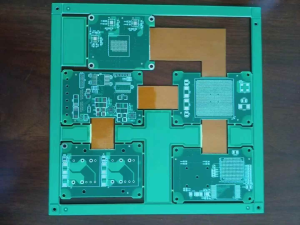
Flexible PCB
1: Flexible PCB Routing Mistakes in the Design Stage
One of the most common pitfalls in flexible PCB development arises during the routing phase. Engineers often apply the same routing mindset used for rigid boards to flexible circuits. This can be disastrous.
Understanding Stress Points in Bends
Unlike rigid PCBs, flexible PCBs operate in environments where they may need to bend, twist, or fold. When traces are routed perpendicularly across bend lines or stacked without consideration for strain relief, mechanical fatigue occurs. This fatigue may not be apparent in early testing but can manifest as micro-cracking during repeated flexing.
Best Practices:
-
Route traces parallel to the bend radius.
-
Use curved traces rather than sharp 90° angles to reduce localized stress.
-
Avoid vias in dynamic flex zones.
In my experience, too many designers neglect to simulate dynamic motion or real-world movement. This oversight stems from siloed workflows—design engineers focus on electrical function without considering mechanical operation. Bridging this gap requires early cross-functional collaboration.
Trace Width and Spacing Misjudgments
Another error is miscalculating appropriate trace width and spacing. Because flexible PCB substrates are more sensitive to heat and mechanical strain, trace density must be carefully managed. Too narrow a trace might heat excessively under load, while overly close spacing could lead to insulation breakdown.
Mitigation Strategies:
-
Employ IPC-2223 standards as a baseline for trace dimensions.
-
Use thicker copper when current requirements demand it.
-
Integrate impedance control for high-speed signals.
In my view, adopting adaptive design rules that respond to flex region stress profiles is essential. Static DRCs (Design Rule Checks) are no longer sufficient in a world where circuits move.
Ignoring Stackup Configuration in Flex Areas
Designers often overlook how stackup thickness impacts flexibility. A symmetrical stackup may work in rigid sections but become unmanageable when the board must bend. Stiffness increases with layer count and material selection—traits often forgotten during design abstraction.
Guidelines:
-
Minimize layers in flex zones to enhance bend capability.
-
Use adhesive-less base materials when feasible.
-
Maintain consistent thickness transitions to avoid mechanical hinge points.
2: Flexible PCB Material Selection and Its Impact on Reliability
Material selection is a foundational decision in the flexible PCB development process, directly affecting the mechanical performance, thermal stability, signal integrity, and overall reliability of the end product. Despite its importance, this area is frequently underestimated or mishandled, often due to cost pressures or limited understanding of material characteristics.
In this chapter, we’ll explore common mistakes related to material choices in flexible PCBs and how these decisions ripple through manufacturing and long-term use. I will also share my perspective on how shifting priorities in cost and performance can misguide critical engineering choices.
Overlooking the Importance of Polyimide in Flexible PCB Structures
Polyimide is the backbone of most flexible PCB substrates due to its excellent mechanical and thermal performance. However, not all polyimides are equal, and substituting with lower-grade variants or polyester-based alternatives can introduce a range of problems.
Typical Failures Include:
-
Warping or dimensional instability at elevated temperatures.
-
Brittle cracks under repeated flexing.
-
Reduced dielectric strength affecting high-speed signal paths.
Best Practices:
-
Choose high-quality, tested polyimide substrates with proven reliability.
-
Consider the environmental conditions (e.g., temperature, humidity, vibration) the product will face.
-
Partner with material suppliers who offer engineering support and data sheets with mechanical cycling and temperature resilience data.
3: FPCBs Layer-to-Layer Registration and Drilling Alignment Errors
Accurate layer-to-layer registration and drilling alignment are critical for any multilayer printed circuit, but these challenges are especially pronounced in FPCBs manufacturing due to the pliability of materials and the tighter tolerances involved. Misalignments in these areas can lead to electrical failures, mechanical weakness, or complete board rejection.
In this chapter, we’ll examine the primary causes of registration and drilling errors in FPCBs manufacturing, and how these issues can be mitigated through design choices, process control, and tooling strategies. I’ll also share thoughts on why these problems are still prevalent, even with modern manufacturing automation.
FPCBs Registration Challenges in Multilayer Stackups
Multilayer flexible PCBs require precise layer alignment to ensure correct interconnectivity between vias and internal traces. However, due to the soft nature of polyimide and the thinness of dielectric films, these layers can stretch, shrink, or distort during processing—especially during lamination cycles.
Common Results of Misregistration:
-
Open circuits due to via pads not lining up with internal signal layers.
-
Crosstalk and impedance mismatches from skewed trace alignments.
-
Partial shorting between layers if registration exposes copper.
Strategies for Mitigation:
-
Use laser alignment systems during lamination for sub-millimeter precision.
-
Include fiducials and tooling holes in your design to assist with mechanical registration.
-
Design with annular rings that tolerate slight offset to avoid via breakout.
In my experience, some registration errors stem not from equipment limitations, but from a mismatch between design tolerances and process capability. Designers must align their expectations with the real-world tolerances of the fabrication shop—and ideally involve the fabricator during early layout review.
Drilling Alignment Errors in FPCBs Fabrication
Unlike rigid boards where layers are dimensionally stable, flexible PCBs are susceptible to movement during drilling. Even a minor shift can misalign the drill point with the intended pad or via location, particularly problematic in high-density interconnect (HDI) boards.
Symptoms of Poor Drill Alignment:
-
Off-center vias that reduce annular ring integrity.
-
Breakout or partial via connection, compromising reliability.
-
Increased risk of inner-layer shorts, especially in fine-pitch BGAs.
Drilling Best Practices:
-
Use laser or vision-guided drilling systems for flexible circuits.
-
Design with larger annular ring diameters than you would for rigid boards.
-
Consider tented or capped vias where necessary to protect against mechanical exposure.
In several projects I’ve been involved in, improper drill compensation was the root cause of recurring open-circuit defects. Adjusting the drill program to account for material stretch post-lamination solved the problem—but only after several failed batches. This underlines the importance of simulation and process-matching before committing to volume production.
Tooling and Fixation Problems Unique to FPCBs
Flexible materials are notoriously difficult to fixture during mechanical processes like drilling, routing, or scoring. If the board isn’t held securely during processing, even the most advanced equipment cannot achieve reliable outcomes.
Causes of Movement During Processing:
-
Insufficient clamping or fixture support on vacuum tables.
-
Use of temporary adhesives that leave residue or lose grip during heat exposure.
-
Incomplete panelization strategies that don’t account for flexibility.
Tooling Solutions:
-
Use of rigid carrier boards to temporarily stabilize the flexible PCB during machining.
-
Application of controlled-release adhesives that maintain alignment without residue.
-
Design inclusion of “tooling rails” or handling frames around the active circuit area.
I’ve found that many small or mid-size fabrication houses overlook investment in advanced tooling systems for flexible PCBs, choosing to adapt rigid board workflows instead. This false economy results in more scrap and lower yields. Standardizing flex-specific fixturing early in the product lifecycle pays off in both quality and repeatability.
Human Factors in Registration and Drilling of Flexible PCB
Even with the best machines, human oversight remains a key factor in registration and drilling errors. Misinterpreted Gerber files, incorrect drill programs, or skipped inspection steps can derail an otherwise sound production plan.
Human Error Risks:
-
Using outdated revision files for drilling.
-
Manually entering incorrect drill offsets into CAM software.
-
Inadequate visual inspection before lamination.
Preventive Actions:
-
Automate data transfer between design and CAM wherever possible.
-
Employ inspection cameras and optical comparators at each key step.
-
Train personnel specifically for flexible PCB workflows, not just general PCB production.
In my opinion, human error in flexible PCB manufacturing is often underestimated. Because flexible boards are less forgiving, small oversights can have a disproportionate impact. Creating a culture of double-checking and specialized training is a worthwhile investment.
4: FPCBs Pad Design and Thermal Management Errors
Pad design and thermal management are critical factors in ensuring both manufacturability and operational stability in flexible PCBs. Due to their thin, heat-sensitive substrates, flexible boards are significantly more prone to damage from improper pad structures or inadequate thermal planning compared to rigid PCBs.
In this chapter, we’ll explore how poor decisions in pad geometry, heat dissipation strategy, and soldering process control contribute to common failure modes. I will also share my reflections on why these issues are often overlooked in the rush to prototype completion or cost reduction.
Inadequate Pad Anchoring in FPCBs Layouts
Unlike rigid PCBs where pads sit on a stable fiberglass base, pads in flexible PCBs are bonded to a pliable polyimide substrate. Without adequate anchoring, pads are vulnerable to lifting, peeling, or complete detachment during assembly or rework.
Typical Symptoms:
-
Pads tearing off during rework or mechanical stress.
-
Solder joints breaking off due to flexing.
-
Delamination at the copper-to-substrate interface.
Design Corrections:
-
Implement anchor stubs or teardrops to strengthen pad connections.
-
Use “extended” pads with fillets to distribute stress more evenly.
-
Apply selective stiffeners in high-risk areas to prevent board flex during assembly.
I’ve observed that many early-stage designs treat pads as isolated features without considering their interaction with the mechanical environment. Good pad design in flexible PCBs isn’t just about electrical connectivity—it’s about mechanical survivability.
Improper Pad Spacing Leading to Bridging or Shorts
Flexible PCB designs, particularly in fine-pitch connectors or compact sensor modules, often push pad spacing to its limit. However, insufficient spacing can cause solder bridging, especially during reflow, leading to electrical shorts and reliability issues.
Failure Modes:
-
Tin whiskers or bridges forming between adjacent pads.
-
Incomplete solder wetting due to insufficient paste mask openings.
-
Shorts under BGA components that escape visual inspection.
Solutions:
-
Maintain IPC-specified minimum spacing based on pitch and solder type.
-
Utilize solder mask-defined pads (SMD) for better control in high-density areas.
-
Simulate solder flow using 3D assembly tools during layout.
It’s a common trap to “cram” components onto a flex design due to space constraints. But every micrometer saved in pad pitch might cost tenfold in post-production repair or redesign. Design for manufacturability, not just for density.
Neglecting Heat Dissipation Requirements in FPCBs
Heat dissipation is a complex challenge in flexible PCBs. Their thin layers and lack of thermal mass make it difficult to spread or dissipate heat effectively. This becomes critical in high-power or LED applications where hotspots can lead to failure.
Heat-Related Issues:
-
Burn-through or warping of the polyimide substrate.
-
Performance degradation of nearby ICs due to localized heating.
-
Melting of adhesive or delamination at solder joints.
Recommended Techniques:
-
Use copper pours or stitched ground planes to distribute heat.
-
Introduce thermal vias near heat-generating components.
-
Integrate heat sinks or attach to external metal housings via thermal interface materials.
In my view, flexible PCB thermal management is an area where simulation and real-world testing must go hand in hand. While thermal FEA (finite element analysis) tools provide useful insight, they often oversimplify the thermal resistance of layered, adhesive-based systems. You must validate results with empirical tests in full system enclosures.
Overheating During Reflow or Hand Soldering of FPCBs
Even a well-designed flexible PCB can be ruined during soldering if the temperature profile is not tightly controlled. Flexible substrates are more sensitive to peak temperature and dwell time than rigid boards, and they deform easily under prolonged thermal stress.
Soldering Pitfalls:
-
Excessive dwell times causing pad lifting or substrate wrinkling.
-
Overheating leading to shrinkage or copper delamination.
-
Improper use of hot air tools damaging adjacent coverlay.
Best Practices:
-
Define specific reflow profiles optimized for the flex layer stackup.
-
Limit rework with hot air to non-critical areas or use pre-heating techniques.
-
Use lower-temperature solders (e.g., Sn-Bi or Sn-In) when possible.
From a systems design perspective, I believe reflow soldering protocols for flexible PCB assemblies should be co-developed with the manufacturer—not retrofitted. Every flex board has unique thermal behavior that cannot be generalized. Creating a custom profile for each design is not a luxury; it’s a necessity.
Underutilizing Thermal Relief Structures in FPCBs Pads
Thermal reliefs are often overlooked in flexible PCBs, especially when designers are more concerned with structural integrity than soldering quality. However, directly connecting a pad to a large copper area without thermal relief can make soldering inconsistent, leading to cold joints or partial reflow.
Common Consequences:
-
Pads failing to reach reflow temperature in time.
-
Inconsistent wetting or tombstoning of small passive components.
-
Manual rework increasing risk of mechanical damage.
Design Solutions:
-
Use spoke-style thermal reliefs around pads connected to large copper areas.
-
Tune the number of spokes and their width based on the current requirement and heat flow.
-
Run DFM (Design for Manufacturability) checks with your assembly partner.
I’ve encountered projects where simply adding thermal reliefs cut soldering failure rates by half—yet the change took only 15 minutes to implement. This reinforces the idea that many flexible PCB failures are entirely preventable with informed design habits.
5: FPCBs Mechanical Damage and Bending Design Errors During Assembly
One of the primary advantages of flexible PCBs lies in their ability to bend and conform to tight enclosures. However, this very property introduces complex challenges during handling, assembly, and post-installation use. Improper mechanical design or careless assembly can easily result in tears, delamination, or trace fractures, many of which are difficult to detect until late-stage product testing—or worse, after deployment.
In this chapter, we analyze common errors related to mechanical handling and bending strategies of flexible PCBs. These issues not only impact product reliability but also increase manufacturing yield loss and field return rates. I’ll also reflect on how early design awareness can prevent irreversible damage and how cross-disciplinary collaboration between mechanical and electrical teams is crucial.
Over-Bending of FPCBs Beyond Minimum Bend Radius
Every flexible PCB has a defined minimum bend radius, typically determined by the substrate thickness, copper layer count, and the specific material properties. Exceeding this limit introduces excessive stress to the copper traces, adhesives, and insulation layers—leading to cracking, micro-fractures, and eventual circuit failure.
Typical Symptoms:
-
Hairline cracks that create intermittent open circuits.
-
Delamination between copper and polyimide.
-
Complete mechanical tearing in high-flex applications.
Prevention Guidelines:
-
Follow IPC-2223 guidelines for minimum bend radius (typically 6-12 times the thickness of the flex stack).
-
Avoid bending along trace paths; always align bends parallel to trace routing.
-
Communicate bend requirements clearly in mechanical drawings and fabrication notes.
In my experience, these failures often occur when designers don’t think about real-world handling. A beautiful layout in CAD becomes a liability if the flex portion must fold like origami inside a housing. Always validate design intent with physical mockups before finalizing the layout.
Lack of Strain Relief Structures in FPCBs Design
Flexible PCBs, particularly in dynamic-flex applications such as printer heads or robotic arms, undergo continuous movement. Without proper strain relief, solder joints at the interface between rigid and flex portions are prone to fatigue, leading to cracked joints and broken traces.
Design Oversights:
-
No stiffener or strain relief at flex-to-rigid transitions.
-
Connectors soldered directly onto unsupported flex zones.
-
Repeated movement concentrated at one edge or corner.
Design Techniques for Mitigation:
-
Add stiffeners or adhesive-backed supports at connector junctions.
-
Use looped flex designs (service loops) to absorb dynamic motion.
-
Avoid placing components too close to the bend area.
One of the most preventable causes of field failure I’ve seen is solder cracking at connector joints due to movement fatigue. Simply adding a Kapton stiffener or adjusting the bend location can extend the flex life of the board dramatically.
Improper Handling of FPCBs During Assembly
Human handling is a surprisingly frequent cause of mechanical failure in flexible PCB manufacturing. Operators may bend or stretch the flex region excessively during component placement, soldering, or inspection. These unintentional movements introduce internal stresses or damage that may not show up until the product is powered on or subjected to vibration testing.
Common Handling Mistakes:
-
Flex circuit hanging unsupported from a clamp or fixture.
-
Excessive force applied during connector insertion.
-
Static pressure from tools causing coverlay deformation.
Handling Best Practices:
-
Use custom fixtures to support the flex during all assembly steps.
-
Implement clear training for operators on flex board sensitivity.
-
Apply visual inspection for creases or dents before moving to the next production step.
In my view, training is the key here. Many SMT technicians are used to handling rigid PCBs and don’t understand how different flex circuits behave. Simple awareness and process controls can reduce handling-related damage significantly.
Unplanned Creasing or Folding of FPCBs in Enclosure Assembly
Creasing—creating a hard, narrow fold in the flex material—is a near-certain path to circuit degradation. It’s often unintentional, happening when installers force the PCB into a tight space without considering the board’s natural bendability. Unlike elastic materials, flexible PCBs do not recover well from sharp folds.
Resulting Failures:
-
Trace fracturing under the crease line.
-
Inner-layer shorts due to compressed dielectric.
-
Cracking of plated vias or SMD solder joints.
Preventive Actions:
-
Design dedicated bend zones with guided arc bends.
-
Avoid sharp enclosures or mating surfaces that pinch the flex.
-
Provide routing documentation to assembly technicians showing bend allowances.
I once worked on a medical wearable where over half of the initial failures were traced to final enclosure assembly. The flex PCBs were functional until they were folded into the plastic shell—where a hidden pinch point created stress that fractured several traces. The fix involved a mechanical design revision, not an electrical one. This demonstrates the deeply intertwined nature of flexible PCB success.
Ignoring Dynamic Flex Testing in Product Validation
Many engineers assume that if a flexible PCB passes initial electrical testing, it’s reliable. But for applications involving motion—such as folding phones, print heads, or aerospace harnesses—static testing is insufficient. Without dynamic flex cycle validation, latent defects can remain hidden until the device is in use.
Consequences of Skipped Testing:
-
Reduced product lifespan due to fatigue cracking.
-
In-field failure during vibration, motion, or shock events.
-
Warranty costs and damage to brand reputation.
Recommended Validation Approaches:
-
Conduct bend cycle testing per IPC-2223 or customer-specific criteria.
-
Use high-speed cameras or electrical monitoring during flex tests.
-
Simulate worst-case bending scenarios based on real-world use conditions.
In my opinion, flexible PCB designs deserve the same mechanical durability scrutiny as structural parts. Unfortunately, this responsibility often falls into the gap between the mechanical and electrical teams. Bridging this gap with integrated validation testing is a best practice that future-proofs product quality.
6: FPCBs Electromagnetic Interference (EMI) and Signal Integrity Design Errors
In modern electronic systems, especially those that involve high-speed digital signals, radio frequency (RF) circuits, or analog-digital coexistence, electromagnetic interference (EMI) and signal integrity (SI) become critical performance concerns. These concerns are magnified in flexible PCB design due to the unique material characteristics, lack of continuous ground planes, and variable impedance in bend regions.
This chapter explores the most frequent EMI and SI errors in flexible PCB design, their real-world consequences, and actionable techniques for mitigation. I’ll also reflect on the systemic gaps between schematic design and layout execution that often allow these issues to slip through unnoticed until late in product development.
Lack of Continuous Ground Plane in FPCBs Designs
One of the most damaging EMI-related errors in flexible PCBs is the absence or fragmentation of the ground plane. Many designers attempt to minimize copper weight to maintain flexibility, inadvertently cutting or segmenting the return paths for high-speed signals.
Typical Issues:
-
Increased loop area leading to higher EMI emissions.
-
Unstable return currents causing cross-talk between adjacent signals.
-
Ground bounce and noise sensitivity in analog sections.
Solutions:
-
Use at least one continuous ground layer across the entire flex region, even in dynamic flex zones.
-
When necessary, use cross-hatched (meshed) ground planes to preserve flexibility while maintaining shielding.
-
Route high-speed signals over uninterrupted ground references.
In my opinion, the myth that “flexible PCBs don’t need ground planes because they’re small” is one of the most harmful misconceptions in layout design. Size doesn’t eliminate the laws of electromagnetism—proper referencing does.
Improper Impedance Control in FPCBs Traces
Signal integrity issues in flexible PCBs often stem from poorly controlled impedance, particularly in differential pairs or single-ended high-speed nets. This becomes increasingly critical as clock speeds rise and edge rates become steeper.
Symptoms of Poor Impedance Control:
-
Signal reflections or overshoot.
-
Increased bit error rates in data transmission.
-
Failure in eye diagram or time-domain reflectometry (TDR) tests.
Preventive Measures:
-
Calculate impedance values using stackup-specific models (considering the dielectric constant, trace width, and spacing).
-
Route differential pairs with consistent spacing and length matching.
-
Engage your PCB manufacturer early to define realistic impedance tolerances in flex zones.
A crucial lesson I’ve learned is that impedance-controlled routing in flexible PCBs must be co-engineered with the fabricator. Flex materials and layer stackups behave differently than rigid ones, and design tools alone don’t always capture the full picture. Always prototype and measure.
Signal Return Path Disruption Across Rigid-Flex Interfaces
In rigid-flex PCBs, where signals transition between rigid and flexible sections, return paths are frequently compromised due to layer changes or ground plane discontinuities. If the return current cannot follow its natural low-inductance path, it will radiate and couple into other systems.
Common Mistakes:
-
Changing layers mid-trace without stitching vias to adjacent ground planes.
-
Routing signals across a flex-rigid boundary with no ground continuity.
-
Placing sensitive analog traces near fast digital signals without isolation.
Design Techniques:
-
Use stitching vias generously when changing layers.
-
Create dedicated ground stitching “curtains” near rigid-flex interfaces.
-
Isolate signal domains (e.g., analog, digital, RF) with segmented ground islands connected at a single point.
From a systems integration perspective, treating the return path with the same priority as the signal path is vital. In projects I’ve advised on, simply adding one or two strategic stitching vias solved months-long EMI failures.
Neglecting Shielding Techniques for Sensitive FPCBs Applications
In some applications—such as medical wearables, automotive electronics, or defense systems—external EMI is a critical threat. Flexible PCBs without proper shielding are vulnerable to noise ingress, which can interfere with sensors, timing circuits, or communication links.
Potential EMI Risks:
-
Electromagnetic susceptibility (EMS) causing erratic system behavior.
-
Failures to meet FCC, CE, or MIL-STD compliance tests.
-
Data corruption in wireless transmission systems.
Recommended Shielding Strategies:
-
Use copper shield layers or mesh with grounded stitching vias.
-
Apply conductive coatings or wraps over finished flex sections.
-
Encapsulate flex sections with metalized films or shielded cables.
There’s a misconception that shielding in flexible circuits is too bulky or cost-prohibitive. However, with modern materials and integrated flex shielding techniques (like Z-axis conductive films), this challenge is solvable without sacrificing form factor. Designers must start considering shielding at the architecture stage, not as an afterthought.
Overlooking Crosstalk and Parallel Routing in FPCBs
Due to tighter routing in compact designs, FPCBss are especially susceptible to crosstalk, where signals in adjacent traces interfere with one another. This is compounded by the absence of interlayer dielectric support and thinner insulation layers.
Signs of Crosstalk Problems:
-
Unexplained signal glitches or noise.
-
Degraded rise/fall times in square waves.
-
Failures in multi-channel communication interfaces.
Crosstalk Mitigation Tactics:
-
Maintain adequate spacing between signal traces, especially between aggressive digital signals and sensitive analog/RF lines.
-
Use ground traces or guard traces between critical nets.
-
Avoid routing high-speed lines in parallel over long distances.
My reflection here is that many SI issues in flexible PCBs don’t arise from routing complexity, but from failing to respect the environment the traces live in. Designers must visualize not only the copper geometry but also the electromagnetic fields that surround them—especially in ultra-compact systems like wearable electronics.
7: FPCBs Masking Layer and Coverlay Application Errors in Manufacturing
In flexible PCB manufacturing, solder mask layers (in rigid-flex areas) and coverlays (in fully flexible zones) play critical roles in protecting circuitry, maintaining insulation, and enhancing mechanical durability. However, improper application of these protective layers is a leading cause of functional and mechanical failure in flexible circuit products.
In this chapter, we examine the most frequent errors in solder mask and coverlay usage in flexible PCBs, highlighting how improper geometry, misalignment, or material selection can compromise performance. I will also share why, from my perspective, designers and fabricators often misunderstand the unique behavior of these layers, treating them with the same logic as rigid PCB processes—an assumption that leads to costly defects.
Incorrect Coverlay Opening Size and Alignment in FPCBs Designs
Unlike solder mask in rigid boards, coverlays are typically pre-cut polyimide films laminated over the copper surface. Misalignments or improperly sized openings can obstruct pads, expose traces, or even delaminate during reflow.
Common Issues:
-
Misalignment between coverlay openings and pads, leading to incomplete solder joints.
-
Pads partially covered, increasing the chance of cold solder joints or bridging.
-
Coverlay edges too close to traces, causing stress points during bending.
Preventive Design Practices:
-
Always oversize the coverlay opening slightly beyond the pad to account for registration tolerance (typically 3–5 mils).
-
Use rounded openings instead of sharp rectangles to prevent tear propagation.
-
Define coverlay layer clearly in the Gerber files and communicate expected tolerances to the fabricator.
In my experience, many engineers treat coverlay openings as if they behave identically to solder mask windows, which is fundamentally flawed. Coverlays require more clearance due to mechanical placement variation and lamination shift. Failing to accommodate this will yield poor soldering and long-term reliability issues.
Overlapping Coverlay and Stiffener Placement Errors in FPCBs
When stiffeners and coverlays overlap or interfere with each other’s boundaries, warping or delamination may occur during reflow or operation. This is especially problematic in connector zones or ZIF (zero insertion force) contact areas, where mechanical tolerances are tight.
Manufacturing Pitfalls:
-
Laminating stiffeners directly on top of coverlay edges, creating step discontinuities.
-
Not allowing sufficient relief zones for adhesive flow during lamination.
-
Misaligned stiffeners causing coverlay bubbling or buckling.
Best Practices:
-
Avoid overlapping coverlay and stiffener edges—leave a small separation gap (0.5–1.0 mm).
-
Define all stiffener and coverlay outlines in the stack-up drawing with separate layers.
-
Use tapered or radius-edged stiffeners to reduce stress concentrations.
From my perspective, this is where layout, mechanical, and process engineering must collaborate early. These interfaces behave more like composite materials than printed circuits, and slight misjudgments in overlap geometry can drastically affect planarity and connector reliability.
Improper Use of Solder Mask Instead of Coverlay in FPCBs Zones
Some designers, often for cost-saving reasons, opt to use solder mask instead of polyimide coverlay in flexible regions. While this may work in simple or static applications, it significantly reduces mechanical integrity in any environment involving bending, vibration, or thermal cycles.
Failure Modes:
-
Cracking of solder mask during flexing.
-
Insufficient adhesion to polyimide substrate.
-
Premature exposure of traces to moisture or contaminants.
Recommendation:
-
Use polyimide coverlay in all dynamic-flex zones or where reliability is mission-critical.
-
Restrict solder mask use to semi-flex or static zones, such as rigid-flex transition areas.
-
If budget is a concern, discuss hybrid solutions with fabricators that selectively apply coverlay only where necessary.
I believe the root of this issue lies in the assumption that all protective layers are interchangeable. But in flexible PCBs, each layer—coverlay, solder mask, stiffener—has a distinct mechanical and thermal role. Shortcutting one layer often weakens the entire structure.
Underspecifying Adhesive Layer Thickness and Flow for Coverlay Lamination
The adhesive layer between the copper and the coverlay (usually acrylic-based) must have sufficient flow characteristics to bond securely without seeping into pad openings or causing surface unevenness. Choosing the wrong adhesive thickness or flow rate leads to reliability problems.
Typical Defects:
-
Delamination under thermal cycling.
-
Excess adhesive flow creating solder mask-like caps over pads.
-
Poor surface planarity affecting component placement.
Lamination Tips:
-
Work with your fabricator to select the right adhesive thickness based on copper topography and pad density.
-
Perform test coupons to validate adhesive coverage and flow under the actual lamination profile.
-
Avoid placing dense pad arrays too close to the coverlay edge to prevent pooling of adhesive.
In my field projects, I’ve seen cases where the board looked perfect—until the customer applied reflow or environmental stress. The coverlay bubbled, and exposed copper oxidized. Postmortem analysis showed incorrect adhesive choice—not the coverlay or copper itself—was the culprit.
Neglecting Thermal Relief Around Coverlay and Mask Cuts in FPCBs
Sharp corners or tight radii in coverlay cutouts act as stress concentrators. When flexed, heat-cycled, or even handled, these points initiate cracking or tearing in the film. Unfortunately, many designers carry over “box-style” pad openings from rigid board layouts, which are unsuitable here.
Design Errors:
-
90-degree coverlay window edges.
-
Tight gaps (<0.1 mm) between cutouts and copper pads.
-
No rounded fillets in flexing regions.
Improved Design Methods:
-
Use oval or rounded rectangular cutouts to distribute mechanical stress.
-
Maintain generous clearance (0.15–0.25 mm) between copper and window edge.
-
Apply finite element simulation (FEM) in high-reliability designs to predict stress points.
From my perspective, the adoption of rounded geometries is one of the most low-effort, high-impact practices in FPCBs design. It not only improves reliability but also makes lamination easier and more consistent across production runs.
8: Common Design for Manufacturability (DFM) Oversights in FPCBs
Design for Manufacturability (DFM) is a critical yet often underutilized principle in flexible PCB design. While most engineers understand DFM in the context of rigid PCBs, FPCBs introduce unique mechanical, thermal, and material behavior that makes DFM even more essential. Ignoring these considerations can result in low yields, unexpected rework, increased costs, and even field failures.
This chapter focuses on common DFM mistakes that occur in flexible PCB design, why they happen, and how they can be prevented. I’ll also provide insights into why bridging the communication gap between designers and manufacturers remains a pivotal challenge in the flexible PCB ecosystem.
Lack of Early Collaboration with FPCBs Fabricators
One of the most frequent—and avoidable—DFM mistakes is failing to involve the fabrication house early in the design process. Flexible PCB manufacturing involves distinct processes, materials, and tolerances that may not align with standard EDA tool defaults.
Consequences of Late Collaboration:
-
Use of materials or layer stacks unavailable from the selected fab.
-
Designs with tolerances tighter than manufacturing capabilities.
-
Repeated design spins due to misunderstood flex/rigid boundaries or coverlay limitations.
Best Practices:
-
Send preliminary stackups and Gerbers to fabricators for DFM review before finalizing the layout.
-
Request material datasheets and design guidelines specific to your fabricator.
-
Leverage DFM checklists that include flex-specific items like stiffener location, bend radius, coverlay opening tolerances, and copper-to-edge clearance.
In my experience, when engineers treat fabricators as late-stage vendors rather than collaborative partners, issues multiply. Early alignment transforms costly trial-and-error into informed, first-pass success.
Violating Minimum Trace Widths and Spacings in Flex Zones
Designers sometimes reuse rigid PCB design rules when laying out traces in flexible regions. However, flexible substrates behave differently—especially under thermal and mechanical stress. Overly narrow traces can crack, and too-close spacing may lead to dielectric breakdown, particularly in high-voltage or high-frequency designs.
Common Symptoms:
-
Cracked copper traces during flexing.
-
Arc-over or shorting in high-voltage environments.
-
Etching inconsistencies due to fine geometries on soft substrates.
Prevention Tips:
-
Confirm minimum trace/space rules with the fabricator for each copper weight.
-
Use wider traces in flex regions, and route them parallel to the bend axis when possible.
-
Avoid placing fine-pitch features near dynamic bend areas.
It’s tempting to push density to the limit, especially in wearables or compact medical devices. But long-term reliability often depends more on mechanical robustness than on packing as many traces as possible into a tight space.
Neglecting Copper-to-Edge Clearance Requirements in FPCBs
FPCBs are often cut with laser, knife, or die methods that exert mechanical or thermal stress on the board edges. If copper traces run too close to the edge, they risk being exposed, lifted, or shorted to conductive surfaces.
Typical Problems:
-
Copper delamination at the edge after singulation.
-
Electrical shorts if exposed traces touch the enclosure.
-
Poor peel strength due to insufficient margin for adhesion.
Design Guidelines:
-
Maintain a minimum of 0.5 mm copper-to-edge clearance in dynamic areas.
-
Increase edge spacing in areas subject to handling, vibration, or enclosure contact.
-
Use protective edge plating or encapsulation when edge contacts are unavoidable.
From a field failure analysis standpoint, edge copper exposure is a silent killer. It may pass testing in pristine lab conditions but fail in the dusty, humid, or metallic environments of real-world usage.
Improper Use of Vias in FPCBs Dynamic Zones
Vias are essential in multilayer PCBs, but in flexible designs—especially in dynamic areas—vias can become points of mechanical stress concentration and early failure.
Common Failures:
-
Cracking around via barrels due to flex cycles.
-
Plating delamination in microvias.
-
Open circuits after mechanical fatigue testing.
DFM-Driven Solutions:
-
Avoid placing vias in areas subject to repeated bending.
-
If unavoidable, use reinforced or teardrop-style pads and vias with larger annular rings.
-
Consider using via-in-pad or buried vias where mechanical durability is critical.
In my opinion, via placement in flex design requires a mechanical-first mindset. You must ask: “What happens to this copper barrel after 1,000 bends?” If the answer is unclear, the layout is not ready for production.
Inadequate Panelization and Assembly Planning for FPCBs
FPCBs are inherently harder to handle in production due to their lack of rigidity. Poor panelization decisions—such as omitting support rails or misplacing fiducials—can lead to misalignment, warping, and low assembly yields.
Assembly-Related Issues:
-
Pick-and-place errors due to inconsistent flex shape.
-
Solder paste misalignment from board movement.
-
Operator mishandling or improper clamping during reflow.
Optimized DFM Approaches:
-
Design rigid panel frames or add detachable rails to assist with SMT assembly.
-
Add global fiducials, tooling holes, and test points that align across the entire panel.
-
Consider using temporary stiffeners or carrier boards for reflow processes.
I strongly advocate for the “design for assembly” mindset, especially when producing FPCBs at scale. You’re not just designing a circuit—you’re designing how that circuit will be built, moved, and inspected.
Failing to Define Layer Stackup and Materials in Fabrication Notes
Some designers assume the fabricator will infer materials and stackups based on industry norms. But in FPCBs, where materials vary widely in thickness, flexibility, and dielectric properties, this assumption often leads to improper builds.
Typical DFM Failures:
-
Use of a different copper thickness than expected, affecting impedance.
-
Missing or misaligned stiffeners due to lack of stackup detail.
-
Incorrect adhesive material or thickness causing delamination.
DFM Best Practices:
-
Always provide a detailed layer stackup, including thicknesses and materials (e.g., polyimide, adhesive, copper weight).
-
Include notes on bend zones, stiffener material, and lamination sequence.
-
Use a fabrication drawing or controlled impedance table if applicable.
In my opinion, treating the fabricator like a black box is a costly design habit. Clear, specific, and complete documentation is the most powerful tool for preventing flex PCB manufacturing defects.
9: Common FPCBs Testing and Quality Control Oversights
No matter how well-designed a flexible PCB may be, failures in testing and quality control (QC) can undermine even the most technically advanced product. Because of the mechanical complexity and sensitive material characteristics involved, FPCBs require more nuanced testing approaches than rigid boards. Skipping or misapplying these steps leads to undetected defects, product recalls, and long-term reliability issues.
This chapter explores the most common quality assurance and testing oversights specific to FPCBs. I’ll also share my own observations on how time pressures and fragmented communication between design, production, and inspection teams often allow critical defects to go unnoticed until after deployment.
Skipping Electrical Continuity and Isolation Testing on FPCBs Panels
One of the most fundamental quality control steps—netlist testing—is sometimes omitted or incompletely performed, especially on prototype runs. For FPCBs, skipping this test increases the risk of sending defective circuits into final assembly.
Consequences of Skipped Testing:
-
Open circuits due to misregistration or drilling errors.
-
Shorts between closely spaced traces caused by solder bridges or etching defects.
-
Inability to isolate field failures from production errors.
Recommended Practices:
-
Use flying probe or fixture-based electrical testing on every panel produced.
-
Match test files with the original netlist from the design database to catch CAM discrepancies.
-
Implement 100% testing on both sides of flex-rigid hybrids, not just the rigid section.
From my view, skipping even one panel in early production can be a fatal mistake. I’ve seen entire product batches rendered useless due to a tiny shift in the via drill program—something a simple continuity test would have caught.
Neglecting Visual and Microscopic Inspection of Coverlay and Pad Quality
Because flexible circuits are often thin, transparent, and prone to handling deformation, visual inspections become more critical than ever. Yet many factories rely only on basic AOI (automated optical inspection), which is tuned for rigid geometries and may miss subtle but dangerous defects.
Commonly Missed Defects:
-
Hairline fractures in traces due to panel warpage.
-
Lifted pads or partial coverlay delamination.
-
Foreign debris or adhesive residue in coverlay windows.
Visual QC Enhancements:
-
Include microscopic or magnified inspection stages (up to 50x) for pad and trace areas.
-
Inspect for bubble formation under coverlay after lamination.
-
Train inspectors to recognize flex-specific surface anomalies like coverlay lift or wrinkling.
I’ve encountered multiple cases where AOI passed a batch, but customers later found soldering failures. Manual microscopic inspection post-lamination caught the root cause—small air pockets beneath pads. AOI isn’t enough in flexible PCB QA; human eyes still matter.
Underestimating the Need for Mechanical Flex Cycle Testing
Electrical testing confirms initial connectivity, but it says nothing about long-term mechanical durability—a defining requirement for most flexible PCB applications. Designs used in wearables, medical probes, or automotive sensors must endure thousands of cycles without performance degradation.
Ignored Risk Areas:
-
Creasing fatigue across folded zones.
-
Copper trace micro-fracturing after dynamic movement.
-
Adhesive breakdown in repeated-use flex areas.
Testing Recommendations:
-
Conduct dynamic bend testing (per IPC-TM-650 or customer-specific cycles).
-
Measure resistance change through cycles to detect early trace damage.
-
Stress test at varying temperatures and humidity conditions for accelerated aging.
From my standpoint, flex PCBs used in real-world movement environments should be tested like moving mechanical parts—not just like static circuits. Many failures emerge only after dozens or hundreds of bending repetitions, well beyond factory test plans.
Failure to Document and Trace FPCBs Quality Data
A key quality control failure in FPCBs production is the lack of traceability. Many facilities lack structured documentation of lot numbers, materials used, inspection results, and test outcomes—especially for small batches or early-stage prototypes.
Consequences of Poor Documentation:
-
Inability to identify systemic issues across builds.
-
No visibility into operator or material root causes for defects.
-
Compliance risk in regulated industries (e.g., medical, aerospace).
How to Improve:
-
Use lot-level traceability with barcodes and database logging of key parameters (e.g., material batches, operator ID, rework events).
-
Store inspection images, resistance logs, and thermal profiles per build.
-
Align documentation standards with IPC-6013 (flex circuits) and ISO 9001/13485 if applicable.
My view is that even small design teams benefit immensely from traceability systems. You don’t need to be a Fortune 500 company to keep a spreadsheet of lamination batches, copper lots, or test results. It’s often the only way to prevent repeat failures.
Inconsistent Standards in FPCBs Quality Judgement
Finally, one of the most overlooked challenges is the lack of consistent standards or criteria for acceptability. What constitutes an acceptable coverlay wrinkle, copper trace nick, or adhesive overflow varies wildly between operators, companies, and even shifts.
Problems Caused by Inconsistency:
-
Disputes between customers and suppliers over rejection causes.
-
Inconsistent yields due to fluctuating inspection pass/fail criteria.
-
Allowing marginal defects that later cause reliability issues.
Solutions for Standardization:
-
Adopt IPC-2223 (Design) and IPC-6013 (Performance) standards as QC benchmarks.
-
Develop photo-based acceptance criteria for common flex defects.
-
Use formal defect libraries and training programs for inspectors.
In my opinion, subjective QC is the enemy of scalable quality. Establishing objective standards—even visual ones—creates consistency, improves yields, and prevents finger-pointing during customer escalations.
10: Common Time and Cost Control Mistakes in FPCBs Production and Delivery
Effective management of production timelines and costs is critical for the success of any FPCBs project. However, the unique complexities of flexible PCB manufacturing often lead to underestimated lead times, overlooked cost drivers, and misaligned supplier expectations. These mistakes can delay product launches, increase expenses, and strain relationships with both customers and vendors.
In this chapter, we will explore the most common errors made during the production and delivery phases of flexible PCBs, analyze their causes, and propose practical approaches to mitigate them. I will also reflect on how project managers and engineers can better coordinate to balance quality, speed, and budget in flexible PCB programs.
Underestimating FPCBs Lead Times Compared to Rigid PCBs
One of the most frequent scheduling errors is assuming FPCBs can be manufactured on the same timeline as rigid boards. The additional steps of coverlay lamination, dynamic testing, and complex stacking inherently extend lead times.
Typical Impacts:
-
Missed product launch dates due to unexpected production delays.
-
Rush orders incurring significant premium costs.
-
Compromised quality due to compressed process windows.
Mitigation Strategies:
-
Plan flexible PCB procurement timelines at least 25-50% longer than rigid PCBs, depending on complexity.
-
Engage fabricators early to understand their current capacity and lead time variability.
-
Factor in additional time for prototype iterations and material qualification.
From my perspective, proactive lead time management is often the difference between a smooth product rollout and a costly scramble. Accepting that FPCBs are not “drop-in” rigid replacements is essential.
Neglecting the Impact of Material Costs and Sourcing Complexities
FPCBs require specialized materials such as polyimide films, flexible adhesives, and stiffeners that are more expensive and sometimes less readily available than rigid PCB laminates. Ignoring this fact can lead to budgeting shortfalls and sourcing delays.
Common Consequences:
-
Unexpected price increases due to global raw material shortages.
-
Production hold-ups while waiting for specialty materials.
-
Cost overruns affecting overall project profitability.
Best Practices:
-
Include a detailed bill of materials (BOM) with pricing contingencies for key flex materials.
-
Develop strong relationships with multiple suppliers to diversify sourcing risk.
-
Monitor market trends for raw materials and forecast demand proactively.
I’ve observed that cost surprises related to FPCBs materials can quickly erode project margins. Early budgeting and supplier engagement reduce this risk considerably.
Failing to Optimize Panelization for Cost and Yield
Because FPCBs are harder to handle, improper panelization can lead to excessive waste, lower yields, and higher per-unit costs. Some teams reuse rigid PCB panelization approaches that don’t translate well to flexible circuits.
Negative Outcomes:
-
High scrap rates due to board deformation or misalignment during assembly.
-
Increased labor costs for manual handling or rework.
-
Difficulty in automated inspection and testing processes.
Optimized Panelization Approaches:
-
Design panels with rigid support rails or tabs to improve rigidity during assembly.
-
Minimize the number of singulation cuts and avoid fragile tabs.
-
Coordinate panel size and fiducials with assembly houses for better automation compatibility.
In my experience, investing time upfront to design flex-optimized panels pays dividends in reduced manufacturing headaches and lower cost per unit.
Overlooking Rework Costs and Their Impact on Schedule
FPCBs are notoriously difficult to rework due to their delicate substrates and thin layers. However, many programs fail to account for rework time and costs during project planning, assuming defects will be minimal.
Rework-Related Risks:
-
Extended lead times as repairs often require manual, time-consuming processes.
-
Higher scrap rates if rework damages adjacent areas.
-
Increased labor costs and technician skill requirements.
Planning Recommendations:
-
Establish realistic rework process capabilities with your fabricator and assembly partner.
-
Implement strict inline inspections to catch defects early and reduce rework volume.
-
Train operators specifically for flexible PCB handling and repair techniques.
From a cost-control standpoint, it’s better to prevent defects than to rely on rework. But when rework is unavoidable, clear planning and specialized skills are essential to prevent schedule slip.
Ignoring the Impact of Testing and Validation Delays
Comprehensive testing—electrical, mechanical, and environmental—is essential for FPCBs but can introduce significant schedule extensions if not planned properly.
Common Delay Factors:
-
Insufficient test resources or equipment availability.
-
Iterative test-fail-fix cycles due to late defect discovery.
-
Overlooked environmental stress tests prolonging validation.
Time Management Strategies:
-
Incorporate test time buffers in project schedules.
-
Parallelize design reviews, prototyping, and test planning early.
-
Use accelerated life testing and simulation tools to shorten validation cycles.
I’ve seen programs where lack of test time planning cascaded into repeated design iterations, causing costly program overruns. Good test planning is a cornerstone of flexible PCB program success.
Poor Communication and Alignment Between Stakeholders
Finally, ineffective communication between designers, fabricators, assembly houses, and project managers often results in mismatched expectations on timing and cost.
Typical Communication Failures:
-
Fabricators not informed about design changes, causing rework.
-
Assembly houses unaware of special handling needs.
-
Project managers unaware of supplier lead-time constraints.
Improvement Measures:
-
Schedule regular cross-functional meetings including all key stakeholders.
-
Use shared project management tools with version-controlled documentation.
-
Establish clear escalation paths for delays or technical issues.
In my view, the human element—clear, timely communication—is as critical as any technical process in avoiding costly flexible PCB production mistakes.
Summary and Final Thoughts on Avoiding Common FPCBs Errors
Throughout this comprehensive guide, we have explored the top 10 common errors in FPCBs manufacturing, including material selection, design pitfalls, process control, assembly challenges, testing, and packaging considerations. Each chapter dissected specific issues and provided actionable best practices aimed at improving reliability, yield, and product performance.
Key Takeaways
-
Materials Matter: Choosing the right substrates, adhesives, and coverlays is foundational to avoiding delamination, cracking, and environmental failures.
-
Design for Flexibility: Incorporate bend radius rules, proper trace and via placement, and component positioning that accommodates mechanical stresses inherent to flex circuits.
-
Process Control is Critical: Rigorous lamination, etching, drilling, and coverlay application controls minimize defects and improve yield.
-
Assembly Requires Specialized Care: Handling, soldering, connector selection, and thermal profiling tailored to flexible PCBs prevent mechanical and electrical failures.
-
Testing and Inspection Must Be Comprehensive: Environmental, mechanical, and electrical testing aligned with product application ensure robustness in the field.
-
Packaging and Shipping Protect Quality: Proper mechanical support, ESD protection, and environmental controls safeguard flexible PCBs through the supply chain.
-
Continuous Improvement Drives Success: Structured quality assurance, failure analysis, and feedback loops enable proactive defect prevention and innovation.
FPCBs manufacturing presents unique challenges distinct from rigid PCB production, demanding a multidisciplinary approach integrating materials science, mechanical engineering, process technology, and quality management. In my experience, collaboration among design, fabrication, assembly, and quality teams is vital to preempt errors and optimize outcomes.
Investing upfront in education, communication, and process discipline not only reduces costly rework and warranty claims but also accelerates time-to-market and enhances customer satisfaction. As flexible electronics continue to proliferate across industries, mastering these best practices is essential for manufacturers and designers aiming to lead in this dynamic field.

- long board pcb
- Flexible PCBs
- Special PCB
- Express Printed Circuit Board
- Pcb Prototype
- LED PCB
- PCB
- Printed Circuit Board
- Pcb meaning
- Pcb manufacturer
- Rigid pcb board
- Rigid Flex PCB
 Quote
Quote
 E-mail