1. Introduction to Counterbores in PCB Manufacturing
Printed Circuit Boards (PCBs) are foundational to all modern electronic devices, from consumer electronics to mission-critical aerospace systems. Within the complex landscape of PCB mechanical and electrical design, counterbores serve as a specific structural feature that facilitates certain mechanical and assembly requirements. Though they may seem like a minor detail, counterbores can significantly influence the board’s mechanical performance, component fitment, and overall assembly process.
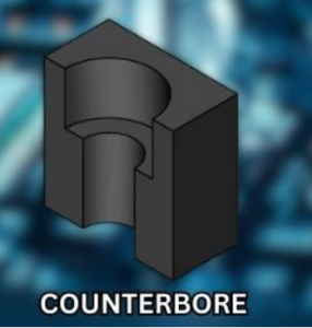
A counterbore is a cylindrical, flat-bottomed recess that is machined around a hole to allow the head of a bolt, screw, or other fastener to sit flush with or below the surface of the board. In PCB manufacturing, these features are especially critical when certain mounting components need a flush surface or when mechanical protection is required for connectors or screw heads.
While the implementation of counterbores is not necessary in every PCB design, they become indispensable in boards designed for mechanical rigidity or those undergoing significant physical interactions. Their utility spans across automotive control units, ruggedized industrial PCBs, and even high-density consumer products where space is limited but mechanical reliability is non-negotiable.
From a design perspective, counterbores add another layer of complexity, as they must be factored into the stack-up, drill file programming, material thickness, and stress analysis. While modern CAD tools make it easier to model them accurately, their incorporation still requires deep knowledge of manufacturing tolerances, substrate mechanics, and tooling capabilities.
counterbore
2. Historical Context of Counterbores in PCB Design
The inclusion of counterbores in PCB design is not a recent innovation. While the practice of recessing mechanical fasteners dates back centuries in general engineering, their adaptation into the printed circuit board industry was driven by the growing need for mechanical-electrical integration during the mid-to-late 20th century. As electronic devices evolved from bulky enclosures to compact, layered systems, mechanical engineers and PCB designers were forced to collaborate more closely. This convergence of disciplines led to the introduction of counterbores as a practical design solution.
In the early stages of PCB development, most boards were single-sided and housed in large mechanical assemblies. Fasteners were used liberally, and the boards themselves were thick enough that surface-mounted or protruding fasteners did not interfere with other components. However, as multilayer boards became commonplace in the 1970s and 1980s—particularly in aerospace and industrial electronics—there was a pressing demand to optimize space usage while maintaining strong mechanical interfaces. This is where counterbores became essential.
Early usage of counterbores was largely mechanical in nature. For instance, when installing heavy-duty connectors or sockets, counterbores ensured that fastener heads wouldn’t protrude and cause stress or clearance issues with enclosures or neighboring components. In some cases, counterbores were added to prevent damage to traces or components during assembly or service. These applications gradually became standardized in military and aerospace specifications, where vibration, shock, and reliability were critical design considerations.
By the 1990s, as consumer electronics grew more compact and sophisticated, counterbores began appearing more frequently in commercial PCB assemblies—though selectively. Their usage spread into telecommunications equipment, automotive ECUs, and even handheld devices. This transition was not just functional; it was also aesthetic. Devices like early mobile phones and PDAs needed flush surfaces to accommodate slimmer profiles, tighter packaging, and durable mechanical fastening without compromising PCB integrity.
Simultaneously, the advent of advanced CAD software enabled PCB designers to model counterbores accurately and incorporate them directly into design files and tooling instructions. As fabrication capabilities improved, the precision and consistency of counterbore creation also advanced. Previously, these features may have required manual intervention or post-processing. With CNC-controlled drills and automated inspection systems, the process became fully integrated into standard PCB production flows.
Interestingly, while some manufacturers leaned heavily into using counterbores for specific applications, others avoided them entirely due to the added cost, complexity, or perceived risk of introducing mechanical stress into layered PCB structures. This created a divergence in industry practice—one where some sectors adopted counterbores as standard engineering practice, while others reserved them for special-purpose or high-reliability systems only.
In summary, the historical emergence of counterbores in PCB design was shaped by a combination of mechanical necessity, technological advancement, and evolving design constraints. They reflect a broader trend in electronics toward higher mechanical precision, denser integration, and hybrid design thinking. Today, while they may be invisible in the final product, counterbores remain a silent but vital detail in countless PCB applications.
4. Counterbores in PCB Manufacturing: Design Principles
Designing counterbores into a PCB is not as simple as drilling a hole and adding a recess. It requires a detailed understanding of mechanical tolerances, board material properties, stack-up considerations, and downstream manufacturing capabilities. Poorly designed counterbores can lead to misalignment, delamination, and even total board failure. This section explores the foundational design principles that engineers must follow to successfully integrate counterbores into their PCB layouts.
4.1 Selecting Appropriate Locations for Counterbores
The first and most critical design consideration is the strategic placement of counterbores. These features should only be used in areas of the PCB where:
-
There are mechanical fasteners or standoffs required.
-
The counterbore will not intersect with internal vias or routing layers.
-
There is adequate spacing from surface-mount components, traces, and edge connectors.
In general, counterbores should be located in mechanically neutral zones—areas where there is minimal electrical congestion. Using mechanical layers in CAD tools, designers can isolate these regions and communicate them clearly to the fabrication team.
Moreover, it is important to ensure that the counterbore location aligns with mechanical components in the enclosure, such as threaded inserts, metal spacers, or grounding structures. Misalignment can lead to assembly problems, or worse, excessive force being applied to sensitive zones of the board.
4.2 Determining Counterbore Depth and Diameter
The depth and diameter of a counterbore depend largely on the type of fastener being used. As a general guideline:
-
Depth should be slightly greater than or equal to the height of the fastener head.
-
Diameter should be slightly larger than the head’s maximum width to ensure easy insertion and alignment.
However, these dimensions must also account for board thickness and layer stack-up. In multilayer PCBs, deep counterbores risk penetrating into internal copper layers or dielectric boundaries. To prevent structural damage, a minimum web thickness should be maintained between the bottom of the counterbore and the next nearest copper or laminate layer—typically no less than 0.3 mm.
Advanced CAD software allows designers to simulate cross-sections of the board to verify these dimensions. Additionally, specifying counterbore dimensions in the mechanical drawing (or in Gerber mechanical layer files) helps the manufacturer apply proper drill and routing instructions.
4.3 Material and Substrate Considerations
Different PCB substrate materials respond differently to the mechanical stress induced by drilling or routing counterbores. For instance:
-
FR-4 is relatively tolerant of standard counterbore operations, but overcutting can delaminate its woven glass structure.
-
High-Tg materials offer better heat resistance during machining but may crack under improper tool paths.
-
Aluminum-core or metal-back PCBs require special tooling to counterbore without damaging thermal layers or conductive cores.
The key is to inform the manufacturer in advance of any non-standard base materials, as these might require slower drill speeds, advanced CNC programming, or alternative tooling strategies.
4.4 Tolerances and Dimensional Control
Precision is essential when dealing with counterbores. Common tolerances for counterbore diameter and depth in PCB manufacturing fall within:
-
±0.05 mm for diameter
-
±0.03 mm for depth
However, depending on the application (e.g., aerospace vs. consumer electronics), tighter tolerances may be required. In such cases, close coordination with the fabricator is necessary to confirm achievable tolerances using their available machinery.
Furthermore, designers must specify reference datums—points or planes from which counterbore measurements are taken. These datums ensure that during both machining and final assembly, the counterbore aligns properly with corresponding hardware.
4.5 Copper Clearance and Pad Isolation
In multilayer PCBs, internal copper layers or plated through-holes near the counterbore region must be isolated to prevent short circuits and maintain board integrity. This is particularly important if the counterbore comes close to internal vias or copper planes.
Designers should:
-
Ensure minimum copper-to-hole clearance is at least 0.5 mm.
-
Avoid placing traces or pads on the same layer directly under a counterbore.
-
Use keep-out zones or custom layer masks in the design tool to avoid accidental routing in these areas.
Neglecting copper clearance could result in shorts, poor insulation resistance, or compromised dielectric properties.
4.6 Stack-Up Planning with Counterbores
When incorporating counterbores into the PCB design, the stack-up must be carefully reviewed. Designers need to ensure that:
-
Counterbores do not compromise critical impedance layers or signal paths.
-
The mechanical strength of the board is maintained by reinforcing nearby layers or using thicker prepregs.
-
Ground or power planes disrupted by counterbores are reconnected using vias or stitched copper.
Stack-up planning is especially important in high-speed PCBs, where return path integrity and reference plane continuity are essential.
Counterbores, when properly designed, can become a seamless part of the PCB that enhances mechanical integrity without sacrificing electrical performance. However, they require careful and deliberate planning, collaboration with fabrication partners, and a deep understanding of the interplay between mechanics and electronics. Rushing or overlooking their implications may lead to costly design re-spins or catastrophic mechanical failures.
5. Counterbores in PCB Stack-up and Material Considerations
Integrating counterbores into a PCB design isn’t just a question of mechanical accommodation—it must be considered in the broader context of the board’s stack-up structure and the materials used. Counterbores physically remove part of the PCB’s top layer(s), which directly impacts the surrounding laminate structure, copper planes, and dielectric layers. Failing to evaluate these interactions can lead to weakened mechanical strength, signal degradation, or even catastrophic failure under load or thermal cycling.
5.1 Understanding PCB Stack-Up and Counterbore Positioning
A PCB stack-up defines how the board is constructed, layer by layer, including copper layers, dielectric insulation, prepregs, cores, and any embedded materials. When a counterbore is introduced, the designer is effectively excavating a vertical section through this sandwich of materials.
Key considerations include:
-
Depth of the counterbore relative to the stack-up thickness
Designers must ensure that counterbores do not encroach into signal or power planes unless explicitly planned. For example, in a 10-layer PCB, counterbores typically affect only the top 1–2 layers. Penetrating deeper may disrupt controlled impedance paths or power distribution networks. -
Compensation for layer removal
If a copper layer is removed or partially cut by a counterbore, rerouting or stitching may be required to maintain signal continuity or shielding effectiveness. -
Layer symmetry
Removing material from one side of the stack-up affects the board’s balance. Asymmetric designs may warp during reflow soldering or under thermal stress. Designers can counter this by mirroring the feature on the opposite side (if possible) or adjusting core and prepreg thicknesses to maintain flatness.
5.2 Interactions with Copper Planes and Traces
When counterbores are used, any copper traces or planes in the affected area must be evaluated for clearance and mechanical isolation. Copper elements too close to a counterbore can cause issues such as:
-
Delamination of copper layers during drilling or routing.
-
Electrical shorts if a screw or metal fixture contacts exposed copper.
-
Degraded signal integrity if critical paths (e.g., high-speed traces) are disturbed by the counterbore’s presence.
To avoid these problems:
-
Maintain a minimum copper-to-counterbore clearance (usually ≥ 0.5 mm).
-
Apply anti-pad rules around the counterbore in internal copper layers.
-
Use non-functional pads in internal layers to add mechanical strength without creating electrical connections near the bore area.
5.3 Substrate Material Suitability for Counterbores
Different substrate materials respond differently to mechanical removal processes such as counterboring:
-
FR-4 (Glass-reinforced epoxy laminate): The most common PCB material, FR-4 is generally compatible with counterbores. However, excessive cutting can fray the glass weave or create delamination zones near bore edges, especially under high humidity or temperature cycling.
-
High-Tg Laminates: These are preferred for high-temperature applications. They maintain better dimensional stability during counterbore machining but can be brittle, requiring slower drill feeds and specialized bits.
-
Ceramic-filled or Metal Core PCBs (MCPCBs): Counterbores in these boards are more challenging due to the presence of aluminum or copper cores. Specialized CNC tooling is required, and the counterbore must be shallow enough to avoid cutting into metal layers, which can cause electrical shorts or compromise thermal performance.
-
Polyimide and Flex-Rigid Boards: In flexible PCBs or hybrid stack-ups, counterbores are often impractical due to the thinness and pliability of the substrate. In rigid sections of flex-rigid designs, shallow counterbores may be possible with extra reinforcement layers.
5.4 Counterbore Adhesion and Resin Recession Effects
Counterbores cut into laminated regions where prepregs are bonded with resin. In poorly controlled environments, this can lead to:
-
Resin recession, where thermal or mechanical stress causes the resin to shrink away from the edge of the counterbore.
-
Poor adhesion of adjacent copper or mask layers, especially if residue remains in the bore after machining.
-
Moisture ingress, since exposed resin in the bore can absorb water and lead to delamination or corrosion.
To mitigate this:
-
Ensure cleanroom drilling and post-processing cleaning of all counterbore features.
-
Use resin-filled or plugged via techniques to seal the area near counterbores.
-
Apply protective surface treatments (e.g., conformal coating or parylene) if counterbores are exposed to environmental elements.
5.5 Effects on Board Warpage and Thermal Expansion
Counterbores affect the board’s mechanical stiffness and local thermal expansion profile, especially in multilayer and large-format boards. Because the machining process removes layers in a concentrated area, thermal stresses during operation or solder reflow can lead to:
-
Localized warping
-
Crack propagation from the bore edge
-
Uneven expansion, potentially damaging components or connectors mounted near the counterbore
Designers can preemptively address this by:
-
Reinforcing surrounding regions with copper pours or stitching vias.
-
Using symmetrical counterbore patterns to balance stress distribution.
-
Selecting low-CTE (coefficient of thermal expansion) materials when operating across wide temperature ranges.
In conclusion, the successful use of counterbores in PCBs is inseparable from proper stack-up planning and material selection. What seems like a simple mechanical recess introduces a cascade of electrical, thermal, and mechanical effects that ripple through the entire board design. By evaluating these interactions early and thoroughly, designers can harness the advantages of counterbores without compromising board integrity or performance.
6. Applications of Counterbores in Specific PCB Markets
The use of counterbores in PCB manufacturing is often application-driven, shaped by industry-specific performance, reliability, and space requirements. While not a universal feature, counterbores offer tangible advantages in sectors where mechanical fastening, flush mounting, or precise component alignment are non-negotiable. This section explores how different markets integrate counterbores into their PCB designs, what benefits they gain, and the trade-offs they accept.
6.1 Counterbores in Consumer Electronics
In compact consumer devices—smartphones, tablets, smartwatches, headphones—space is a premium. Counterbores are used to:
-
Mount micro screws or threaded inserts without increasing thickness
-
Align plastic or metal enclosures flush with the board surface
-
Secure small mechanical modules, such as camera mounts or haptic motors
Design Benefit:
Flush mechanical integration enhances product appearance, reduces edge snagging, and supports miniaturization.
Example:
A smartwatch PCB may include four micro counterbores near the perimeter to receive screws that anchor the frame. These features allow for a seamless external profile while ensuring robust internal structure.
6.2 Counterbores in Automotive Electronics
In the automotive sector, vibration, thermal cycling, and moisture are constant challenges. Counterbores are frequently employed in:
-
Engine control units (ECUs)
-
Advanced driver-assistance systems (ADAS)
-
Battery management systems (BMS)
Purpose of Counterbores:
-
Secure mounting of heavy connectors that need reinforcement
-
Grounding through metal screws that require embedded bushings within the PCB
-
Avoidance of protrusions that might interfere with enclosure seals
Reliability Advantage:
Counterbores help reduce stress concentration around holes and ensure consistent torque application during assembly, both of which improve long-term reliability in harsh environments.
6.3 Counterbores in Industrial and Robotics Applications
Industrial electronics often demand modular design, mechanical ruggedness, and replaceability. Counterbores play a critical role in:
-
Mounting PCBs to DIN rails or aluminum frames
-
Attaching motors, sensors, or relays directly to the board
-
Withstanding high-torque forces from attached components
Use Case:
A PCB in a robotic actuator system may use counterbores to mount the board directly onto a moving armature. These counterbores provide mechanical robustness while avoiding excessive height that would interfere with actuator movement.
Special Consideration:
To withstand industrial abuse, PCBs with counterbores in this context often use high-Tg materials, edge plating, or thicker copper weights to reinforce structural integrity.
6.4 Counterbores in Aerospace and Defense Systems
Few industries have tighter tolerances and higher reliability demands than aerospace and defense. Counterbores are used in:
-
Flight control boards
-
Satellite telemetry systems
-
Missile guidance electronics
Why Counterbores Matter Here:
-
Flush-mounting of components to minimize vibration under G-forces
-
Physical coupling of heat sinks to board through metal standoffs
-
High-precision mechanical alignment critical to optical or RF subsystems
Example:
A radar control PCB may use counterbores to precisely align with metal brackets that house sensitive RF modules. Even small misalignments can degrade signal performance, so the counterbores must meet stringent tolerances.
Downside:
Tight specifications require additional inspection steps, including 3D metrology and X-ray analysis, increasing cost and production time.
6.5 Counterbores in Medical Devices
In medical electronics, especially implantables or diagnostic tools, space-saving and mechanical precision are vital. Counterbores are used in:
-
Portable diagnostic tools
-
Handheld ultrasound equipment
-
Wearable biosensors
Function:
-
Allow internal fastening of enclosures without protruding hardware
-
Align PCB components with external interfaces (USB ports, screens, etc.)
-
Reduce snag points that could interfere with surgical or patient environments
Material Consideration:
Boards used here often feature biocompatible conformal coatings, and counterbores must be machined without introducing particulate contamination or microcracks.
Regulatory Implication:
Because medical devices are subject to FDA and ISO certifications, the counterbore process must be thoroughly documented and validated as part of the product lifecycle.
6.6 Counterbores in Telecom and Networking Equipment
Large-scale telecom and networking systems—such as base stations, server blades, and switching routers—use PCBs that support heavy components, like heat sinks or fiber modules.
Counterbores Enable:
-
Flush installation of metallic brackets or grounding bars
-
Mechanical isolation of vibration-sensitive optical modules
-
Secure and precise installation of modular components
High-Volume Example:
In a high-speed backplane, counterbores allow daughterboards to be screwed into precise positions without violating height constraints or airflow channels. This ensures consistent impedance and mechanical connectivity.
6.7 Counterbores in LED Lighting and Power Electronics
LED drivers, high-power supply units, and industrial lighting modules rely heavily on thermal management. Counterbores are often incorporated to:
-
Anchor metal heat sinks directly to the PCB surface
-
Ensure firm screw contact with internal copper planes for grounding and heat transfer
-
Allow mechanical fastening without compromising thermal interface materials (TIM)
Counterbores are not a niche mechanical feature—they are a strategic design element found across a wide spectrum of industries. Whether optimizing for space, strength, or signal performance, their role is indispensable in applications where mechanical-electrical integration must be seamless, robust, and repeatable. Each market tailors its use of counterbores according to its specific demands, demonstrating the versatility and engineering importance of this feature in modern PCB manufacturing.
7. Future Trends and Innovations in Counterbore Technology for PCBs
As PCB manufacturing technology advances, the use and execution of counterbores continue to evolve, driven by demands for higher precision, miniaturization, and integration of multifunctional features. Emerging trends and innovations are shaping how counterbores will be designed, fabricated, and utilized in next-generation electronics. This section explores these developments and their potential impact on the PCB industry.
7.1 Automation and AI-Driven Counterbore Fabrication
-
Smart CNC Systems: Advanced CNC drilling and routing machines increasingly incorporate AI algorithms for adaptive cutting, automatically adjusting feed rates and tool paths in real time to optimize counterbore quality and reduce tool wear.
-
Predictive Maintenance: AI-powered sensors monitor tooling condition and machine health, predicting when tools need replacement before defects occur, improving yield and lowering downtime.
-
Automated Inspection: Machine vision systems enhanced with deep learning identify subtle defects such as micro-burrs or depth inconsistencies in counterbores, enabling 100% inline inspection and reducing manual QC efforts.
7.2 Advanced Materials and Additive Manufacturing
-
New PCB Substrates: Emerging high-performance substrates such as polyimide composites, ceramic-based laminates, and flexible materials challenge traditional counterbore machining methods due to their hardness or flexibility. Specialized tools and techniques, such as ultrasonic drilling and laser machining, are becoming essential.
-
Additive Manufacturing Integration: Combining subtractive counterbore machining with additive processes like selective laser sintering (SLS) or inkjet printing may enable on-demand fabrication of integrated mechanical features, reducing post-processing and assembly steps.
Conclusion: Final Thoughts on Counterbores in PCB Manufacturing
Counterbores play a crucial yet often understated role in modern PCB manufacturing, bridging the gap between mechanical robustness and electrical functionality. Through this comprehensive exploration, it is clear that counterbores are far more than simple recesses—they are precision-engineered features that demand careful design, precise fabrication, and rigorous quality control.
By integrating counterbores thoughtfully, engineers can achieve:
-
Enhanced mechanical strength and reliability, ensuring secure fastening and improved resistance to vibration, shock, and thermal stresses.
-
Optimized assembly processes, allowing flush mounting of hardware and minimizing product profiles for compact devices.
-
Maintained electrical integrity, when counterbores are designed to avoid critical routing areas and signal-sensitive zones.
The challenges associated with counterbores—such as tooling complexity, tighter tolerances, and potential electrical trade-offs—are surmountable through early collaboration between design and manufacturing teams, adherence to best practices, and the use of advanced equipment and inspection methods.
Looking ahead, the evolution of counterbore technology promises to unlock new capabilities, from AI-assisted fabrication and micro-scale precision to multifunctional embedded features and sustainable manufacturing practices. These innovations will continue to enhance the value of counterbores, making them indispensable in the increasingly demanding landscape of PCB applications spanning consumer electronics, automotive, aerospace, medical, and beyond.
In essence, mastering the art and science of counterbores empowers PCB designers and fabricators to create assemblies that are not only electrically sound but also mechanically resilient and future-ready—a true hallmark of excellence in electronics manufacturing.

- long board pcb
- Flexible PCBs
- Special PCB
- Express Printed Circuit Board
- Pcb Prototype
- LED PCB
- PCB
- Printed Circuit Board
- Pcb meaning
- Pcb manufacturer
- Rigid pcb board
- Rigid Flex PCB
 Quote
Quote
 E-mail