Introduction to Copper Thieving in PCB Manufacturing
Copper thieving in PCB manufacturing is a specialized design technique aimed at improving plating uniformity by adding additional copper patterns—commonly called “thieving patterns”—in areas of the PCB where copper density is low. These patterns are typically non-functional, meaning they are not connected to any circuit or signal paths but are placed solely to balance the copper distribution across the PCB panel. In modern PCB production, achieving uniform copper distribution is critical to avoid issues like uneven plating thickness, warping, and other manufacturing defects.
Copper thieving in PCB manufacturing has become an essential design consideration, particularly as PCB designs grow increasingly complex with finer lines, smaller features, and higher layer counts. In such designs, the absence of uniform copper areas can lead to various electrochemical and mechanical stresses during plating and etching processes. Copper thieving offers an elegant solution to mitigate these risks, although it comes with its own set of challenges and trade-offs.
The Core Motivation for Copper Thieving in PCB Manufacturing
One of the primary motivations for using copper thieving in PCB manufacturing is to control the distribution of current density during the electroplating process. When the copper layout is uneven, areas with less copper experience faster plating, while areas with higher copper density tend to plate more slowly. This results in thickness variations that can compromise both the structural integrity and electrical performance of the PCB. Copper thieving helps balance these current densities by providing additional copper where it is otherwise sparse.
Beyond plating concerns, copper thieving in PCB manufacturing also plays a role in minimizing mechanical deformation. PCBs with uneven copper distribution can warp during lamination, soldering, and reflow processes. By strategically adding copper thieving patterns, manufacturers can achieve a more balanced stress distribution across the PCB surface, reducing the likelihood of warpage and related defects.
Copper Thieving as a Design Element in PCB Manufacturing
Copper thieving is not just a fabrication remedy but an integrated design element in the PCB manufacturing process. Designers must work closely with manufacturers to ensure that the copper thieving patterns are compatible with signal integrity, electromagnetic compatibility (EMC), and thermal management requirements. Poorly designed copper thieving patterns can inadvertently introduce capacitive coupling or unwanted signal reflections, especially in high-speed PCB designs.
Despite its critical importance, copper thieving in PCB manufacturing is often underappreciated during the early stages of design. Many design engineers focus primarily on routing, impedance control, and component placement, sometimes neglecting the effects of copper balancing. However, with increasing PCB layer counts, tighter tolerances, and more demanding applications, copper thieving has gained prominence as a key design and manufacturing parameter.
Evolution of Copper Thieving Practices in PCB Manufacturing
Historically, copper thieving was implemented manually or using simple geometric fills that served to add copper in low-density areas. With the advancement of design automation tools, copper thieving in PCB manufacturing has become far more sophisticated. Modern design software can automatically detect areas of low copper density and generate optimized thieving patterns that comply with design rules and manufacturing tolerances.
Moreover, as PCB applications evolve into high-frequency and high-power domains, the strategy for copper thieving in PCB manufacturing has also evolved. It is no longer sufficient to merely add copper arbitrarily; instead, copper thieving patterns must be carefully considered to ensure they do not interfere with signal traces, vias, or thermal paths. This complexity underscores the growing importance of incorporating copper thieving strategies into early design reviews and simulations.
A Balanced Perspective on Copper Thieving in PCB Manufacturing
The role of copper thieving in PCB manufacturing is inherently a balancing act. On one hand, it offers undeniable benefits in improving plating uniformity, mechanical stability, and overall fabrication yield. On the other hand, it introduces potential design risks, including signal integrity challenges and electromagnetic interference issues if not properly managed.
In this comprehensive exploration of copper thieving in PCB manufacturing, we will delve into both the advantages and disadvantages, review detailed case studies, and discuss best practices for successful implementation. Throughout the article, we will critically assess when copper thieving is essential and when its application may introduce more problems than it solves.
Additionally, I will incorporate my own reflections on the subject, drawn from practical experiences and theoretical evaluations, aiming to present a well-rounded view that extends beyond the textbook explanations.
Copper Thieving
Historical Context of Copper Thieving in PCB Manufacturing
The history of copper thieving in PCB manufacturing is closely tied to the evolution of printed circuit board technologies themselves. As PCBs advanced from simple, single-layer boards to complex, multi-layer and high-density interconnect (HDI) structures, the need for more precise plating and uniform copper distribution became increasingly apparent. Initially, PCB manufacturers faced significant challenges related to uneven copper deposition, warping, and structural inconsistencies. Copper thieving emerged as a practical solution to address these challenges, evolving steadily alongside manufacturing techniques and design requirements.
Early Manufacturing Limitations Leading to Copper Thieving in PCB Manufacturing
In the early days of PCB manufacturing, processes were relatively primitive. Plating methods were less controlled, copper layers were thicker, and design geometries were not as intricate as they are today. During this period, copper distribution across a PCB panel was not a major concern because the designs were inherently more uniform, often due to larger component footprints and less dense circuit routing.
However, as circuit designs became more compact and application demands grew more stringent, uneven copper distribution began to surface as a significant problem. PCB areas with sparse copper would plate faster, leading to inconsistent thickness across the panel. This thickness variation could result in several downstream issues, including etching problems, via integrity concerns, and assembly complications.
To combat these inconsistencies, PCB manufacturers began experimenting with adding “dummy” copper areas—what would later be formalized as copper thieving. Initially, this was done manually by adding copper patches to artwork films used in photolithography. Though effective, this process was labor-intensive and lacked the precision necessary for more advanced applications.
Standardization of Copper Thieving in PCB Manufacturing Practices
As PCB manufacturing matured during the 1980s and 1990s, the industry began to develop more formalized approaches to copper thieving in PCB manufacturing. Fabrication guidelines began to include recommended copper density ratios across the panel to minimize plating anomalies. As a result, copper thieving became a standardized part of the design-for-manufacturing (DFM) checklist.
Design automation tools also began to incorporate copper thieving features, allowing designers to automatically populate low-density areas with carefully spaced copper patterns. These tools reduced the reliance on manual adjustments and improved the overall consistency of copper distribution across PCB panels.
The increasing adoption of surface-mount technology (SMT), which allowed for more compact designs, further emphasized the importance of copper thieving in PCB manufacturing. The thinner traces and smaller components associated with SMT heightened the sensitivity of PCBs to plating and warpage issues, making the careful implementation of copper thieving essential.
The Rise of High-Speed and High-Density PCB Designs
The late 1990s and early 2000s saw the rapid growth of high-speed digital circuits, high-frequency RF boards, and multi-layer PCB assemblies with microvias and buried vias. These advancements introduced new performance requirements, including tight impedance control and reduced electromagnetic interference.
Copper thieving in PCB manufacturing now had to address not just plating uniformity but also electrical performance considerations. Designers had to ensure that thieving patterns would not inadvertently affect signal integrity or create parasitic capacitance that could disrupt high-speed signals. Consequently, the placement, size, and spacing of copper thieving patterns became more sophisticated.
Recent Technological Developments in Copper Thieving for PCB Manufacturing
Modern PCB manufacturing has further refined the role of copper thieving. Advanced computer-aided design (CAD) and computer-aided manufacturing (CAM) tools can now automatically generate highly optimized copper thieving patterns that adhere to strict design rules. These tools take into account factors such as proximity to high-speed signal lines, potential coupling with power planes, and thermal conductivity requirements.
Additionally, the introduction of flex and rigid-flex PCBs has created new challenges and opportunities for copper thieving in PCB manufacturing. Flex circuits, for example, are particularly sensitive to mechanical stresses, making copper balancing crucial to preventing deformation during bending and folding.
As environmental sustainability becomes an increasing focus in the electronics industry, there is also growing attention on optimizing copper usage to reduce waste. Copper thieving, when intelligently applied, can contribute to more efficient material utilization across PCB panels.
Historical Summary and Impact on Modern Manufacturing
Looking back, the historical journey of copper thieving in PCB manufacturing reflects the industry’s continuous pursuit of precision, reliability, and performance. What began as a simple, manual workaround to address plating issues has evolved into a vital, integrated design strategy supported by sophisticated software and robust manufacturing standards.
While the core purpose of copper thieving—achieving plating uniformity—has remained consistent, the complexity of its implementation has grown in parallel with the increasing demands placed on PCBs. Today, copper thieving is no longer an afterthought but a carefully engineered feature that significantly impacts both the manufacturability and performance of advanced circuit boards.
In the following sections, we will explore the technical principles, benefits, and drawbacks of copper thieving in PCB manufacturing in greater depth, including practical examples, best practices, and the latest trends shaping its future.
Purpose and Fundamentals of Copper Thieving in PCB Manufacturing
Copper thieving in PCB manufacturing serves a highly specialized but critical purpose: to balance the copper distribution across the entire printed circuit board panel. Without proper copper balance, manufacturers can encounter a variety of process-related defects that compromise both the structural integrity and the electrical performance of the final product. In this section, we will carefully examine the fundamental reasons for implementing copper thieving, its functional mechanisms, and the key design principles that guide its effective use.
Why Copper Thieving in PCB Manufacturing is Necessary
The primary purpose of copper thieving in PCB manufacturing is to correct copper density imbalances that naturally occur due to circuit layout variations. Some areas of a PCB may be densely packed with copper traces, ground planes, and power connections, while others may be relatively sparse or even empty. This non-uniformity can cause significant issues during several key manufacturing steps, most notably electroplating.
During electroplating, areas with less copper tend to attract more plating current, causing them to accumulate copper more rapidly. Conversely, areas with dense copper features receive less plating current, leading to thinner copper deposition. The result is an uneven surface with variable copper thicknesses across the panel. This can lead to etching difficulties, poor solderability, via quality issues, and even mechanical failures during assembly.
By introducing copper thieving patterns—small, non-functional copper patches or grids—manufacturers can artificially increase the copper density in sparse areas, thus promoting plating uniformity across the entire PCB. Copper thieving effectively controls the current density during plating, helping to ensure consistent copper thickness and improved product reliability.
The Electrochemical Principle Behind Copper Thieving in PCB Manufacturing
The effectiveness of copper thieving in PCB manufacturing is based on Faraday’s Law of Electrolysis, which governs the relationship between current, time, and material deposition during electroplating. Simply put, the amount of copper deposited on a given area is directly proportional to the current it receives.
When copper density is uneven, current tends to flow preferentially to the areas with the least resistance—usually the areas with less copper. These regions plate faster because the local current density is higher. By strategically placing copper thieving patterns, designers can reduce this disparity by balancing the electrical field distribution across the PCB panel, ensuring that all areas plate more uniformly.
This electrochemical principle is foundational to understanding why copper thieving is not merely a mechanical or cosmetic addition but a necessary process control mechanism that directly influences manufacturing quality.
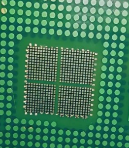
Basic Types of Copper Thieving Patterns in PCB Manufacturing
There are several common patterns used for copper thieving in PCB manufacturing, each with its own design advantages:
-
Square Grid Pattern:
A uniform array of small copper squares evenly spaced across the thieving area. This is the most commonly used and provides excellent control over plating uniformity. -
Circular Dots:
Round copper pads that help minimize sharp edges and reduce the risk of electromagnetic interference. -
Crosshatch Mesh:
A fine, woven grid that offers both copper balance and some degree of flexibility for flex-rigid boards. -
Isolated Copper Islands:
Small, standalone copper areas that offer minimal coupling with surrounding circuitry.
The selection of a copper thieving pattern depends on several factors, including PCB design density, electrical performance requirements, and the specific capabilities of the manufacturer.
Key Design Parameters for Copper Thieving in PCB Manufacturing
When incorporating copper thieving into a PCB design, several critical parameters must be carefully controlled:
-
Minimum Clearance from Signal Traces:
Copper thieving should maintain a safe distance from active signal paths to avoid parasitic capacitance or unwanted coupling. -
Pattern Density:
Over-thieving can lead to excessive copper accumulation and potential signal integrity issues, while under-thieving may not resolve plating problems. -
Pattern Size:
The size of individual copper thieving features must comply with the manufacturer’s minimum feature size and spacing capabilities. -
Copper Distribution Ratio:
Designers typically aim for a copper distribution that does not exceed a predefined maximum-to-minimum density ratio, usually specified by the PCB fabricator. -
Layer Specificity:
Copper thieving patterns may need to vary between layers in multi-layer PCBs to balance copper throughout the entire stack-up, not just on the outer layers.
Integration of Copper Thieving in PCB Manufacturing Workflow
Copper thieving is typically introduced during the design-for-manufacturing (DFM) phase, where PCB designers and fabricators collaborate to ensure the final board can be produced reliably. Modern PCB design tools often include automated copper thieving functions that can quickly identify low-density areas and generate appropriate patterns based on pre-set design rules.
The final copper thieving layout is then reviewed during design verification to ensure it does not interfere with controlled impedance, signal paths, or thermal management requirements. Manufacturers also perform checks to verify that the copper thieving patterns meet their processing tolerances and do not introduce plating or etching complications.
Summary of Copper Thieving Fundamentals in PCB Manufacturing
The use of copper thieving in PCB manufacturing is both a technical necessity and a design art. It serves to balance electroplating currents, reduce mechanical stress, and promote uniform copper distribution across the PCB panel. When properly implemented, copper thieving can significantly enhance product yield, reliability, and performance.
However, copper thieving must be carefully integrated into the design process, taking into account electrical, thermal, and manufacturing constraints. Poorly designed thieving patterns can introduce more problems than they solve, particularly in high-speed, high-frequency, or high-density circuit boards.
In the next section, we will begin exploring the advantages and specific benefits of copper thieving in PCB manufacturing, starting with how it improves plating uniformity and overall process consistency.
Materials and Patterns Used for Copper Thieving in PCB Manufacturing
The selection of materials and patterns is a critical consideration in the successful implementation of copper thieving in PCB manufacturing. While copper thieving primarily focuses on the geometric distribution of non-functional copper areas, the choice of materials, pattern types, and spacing strategies directly influence the effectiveness and safety of the design.
In this section, we will explore the materials commonly used, the variations in copper thieving patterns, and the design factors that contribute to the overall manufacturability and electrical reliability of PCBs.
Copper as the Core Material in Copper Thieving for PCB Manufacturing
Unsurprisingly, the primary material used in copper thieving in PCB manufacturing is copper itself. However, the type and thickness of the copper layer must align with the overall PCB stack-up specifications.
Key copper material considerations include:
-
Copper Foil Type:
Most PCBs use electrodeposited (ED) copper or rolled annealed (RA) copper. For copper thieving, ED copper is more commonly used due to its compatibility with mass production and standard plating processes. -
Copper Thickness:
The thickness of the copper thieving areas is typically the same as the signal layer copper, often ranging from 0.5 oz to 2 oz per square foot, depending on design requirements. This uniformity helps achieve balanced plating across the panel. -
Surface Finish:
Copper thieving patterns may receive the same surface treatments (e.g., HASL, ENIG, OSP) as the functional copper, especially when applied on outer layers. This ensures consistent processing during solder masking and assembly. -
Material Compatibility:
For multi-layer PCBs, the dielectric material surrounding the copper thieving must be compatible with the copper plating and etching processes to avoid delamination or process failures.
In all cases, copper thieving in PCB manufacturing does not introduce foreign materials to the design; it merely optimizes the distribution of the copper already being used.
Common Copper Thieving Patterns in PCB Manufacturing
The effectiveness of copper thieving in PCB manufacturing depends not only on the presence of copper but also on the pattern chosen. Different copper thieving patterns are selected based on design intent, electrical sensitivity, and manufacturing capabilities.
1. Square Grid Pattern
This is the most commonly used copper thieving structure, where small copper squares are evenly spaced in a grid-like arrangement across low-density areas.
Advantages:
-
Provides excellent plating uniformity.
-
Simple to generate using most PCB CAD software.
-
Easy for fabricators to process.
Design Tip:
Maintain a uniform distance between copper squares and critical signal lines to prevent coupling.
2. Circular Dot Pattern
In this approach, small round copper dots are used instead of squares.
Advantages:
-
Minimizes sharp edges, reducing electromagnetic emission risks.
-
Provides smooth copper distribution without aggressive capacitive loading.
Design Tip:
Circular patterns are especially useful near sensitive analog or RF circuits to avoid unwanted coupling.
3. Crosshatch Mesh Pattern
This pattern consists of interconnected lines that form a fine mesh.
Advantages:
-
Balances copper well in large open areas.
-
Provides flexibility for flex or rigid-flex boards, reducing stress concentration points.
Design Tip:
In rigid-flex PCBs, crosshatch copper thieving can improve mechanical bendability.
4. Isolated Copper Islands
These are small, standalone copper features that provide copper balance without forming continuous shapes.
Advantages:
-
Reduces risk of unintentional current paths.
-
Offers minimal interaction with adjacent signal layers.
Design Tip:
Used in areas where cross-coupling or electromagnetic interference must be strictly minimized.
Key Copper Thieving Design Parameters in PCB Manufacturing
When implementing copper thieving in PCB manufacturing, it is crucial to maintain strict control over several design parameters to ensure the patterns deliver the intended benefits without introducing new risks.
-
Copper Feature Size:
Typically ranges from 0.25 mm to 1 mm, depending on PCB fabrication capabilities. -
Spacing Between Features:
Adequate spacing (usually 0.5 mm to 1 mm) prevents excessive copper accumulation and minimizes electrical interaction with adjacent circuits. -
Minimum Distance from Active Traces:
Copper thieving patterns must maintain a clearance (commonly 0.5 mm or more) from active signal lines to prevent unwanted capacitive coupling or impedance changes. -
Layer-Specific Requirements:
In multi-layer boards, copper thieving may vary by layer to balance the overall stack-up rather than just surface layers. -
Consistency Across the Panel:
Copper thieving density should aim to equalize copper distribution across the entire PCB panel, not just isolated areas.
Materials and Pattern Selection Based on PCB Type
The selection of copper thieving patterns in PCB manufacturing can vary significantly depending on the PCB’s intended application and construction type.
-
Rigid PCBs:
Favor square grid or circular dot patterns for ease of manufacturing and consistent plating results. -
High-Speed PCBs:
Require carefully spaced circular dots or isolated islands to prevent signal degradation. -
RF PCBs:
Prefer minimal thieving near RF lines and use low-density circular patterns if copper balancing is essential. -
Flex and Rigid-Flex PCBs:
Often employ crosshatch meshes to balance copper while preserving flexibility. -
High-Density Interconnect (HDI) PCBs:
Use tightly controlled copper thieving with sophisticated design rules to prevent signal and thermal issues in densely packed layers.
The Pros of Copper Thieving in PCB Manufacturing
Copper thieving in PCB manufacturing provides multiple advantages that significantly improve both the manufacturing process and the reliability of the final product. These benefits are especially crucial as PCBs become increasingly complex, with tighter design tolerances, higher layer counts, and more advanced electrical requirements. In this section, we will explore the key pros of copper thieving in PCB manufacturing, highlighting why it has become a valuable tool in modern circuit board production.
Improved Plating Uniformity Through Copper Thieving in PCB Manufacturing
One of the most significant benefits of copper thieving in PCB manufacturing is its ability to enhance plating uniformity across the entire panel. Uneven copper distribution causes areas with low copper density to attract higher current during electroplating, resulting in excessive copper buildup. Conversely, densely populated copper areas tend to plate more slowly.
Copper thieving introduces additional copper in sparse regions, which balances the current density during electroplating. This leads to consistent copper thickness across all areas of the PCB, reducing the risk of plating defects such as thin traces, under-plated vias, and irregular copper surfaces.
Uniform plating improves the reliability of signal pathways, ensures stable mechanical connections, and enhances the overall quality of the PCB.
Enhanced Dimensional Stability with Copper Thieving in PCB Manufacturing
Copper density variations can cause mechanical stress imbalances across the PCB panel during the fabrication process. These stress differences can lead to warpage, bowing, and twisting—issues that may worsen during soldering, thermal cycling, or reflow assembly.
By using copper thieving to balance copper distribution across the panel, manufacturers can achieve better dimensional stability. A well-balanced PCB is less likely to deform during processing or end-use, which is critical for multi-layer, large-format, or rigid-flex boards that are particularly sensitive to warping.
This mechanical stability directly contributes to improved assembly yields and long-term reliability.
Reduction of Localized Electrochemical Stress in PCB Manufacturing
Localized areas with low copper coverage tend to attract higher plating current densities, which can introduce electrochemical stress and plating anomalies such as nodules or excessive growth in specific regions.
Copper thieving reduces the likelihood of these localized electrochemical imbalances by spreading the plating current more evenly across the board surface. This minimizes defects such as over-plating, rough surface finishes, or dendritic growth that can compromise the quality and durability of the PCB.
Improved Manufacturing Yield with Copper Thieving in PCB Manufacturing
Inconsistent copper plating, warpage, and etching defects can lead to high scrap rates and rework during PCB production. By effectively implementing copper thieving, manufacturers can significantly improve process stability and reduce failure rates.
The result is higher overall manufacturing yield, lower production costs, and better throughput. This is especially important in high-volume production runs where small improvements in yield can have a substantial financial impact.
Compatibility with Modern Automated Design Tools
Modern PCB CAD and CAM software platforms often include automated copper thieving generation features. These tools can intelligently detect areas with low copper density and automatically populate appropriate thieving patterns while respecting the required clearances and design constraints.
This automation allows designers to efficiently integrate copper thieving into complex layouts without excessive manual effort. It also helps to standardize thieving patterns across projects, reducing variability between design teams and fabrication partners.
The compatibility with design automation significantly streamlines the design-for-manufacturing (DFM) process, saving time and reducing human error.
Contribution to Balanced Etching in PCB Manufacturing
Copper density directly affects the etching process. During etching, areas with sparse copper tend to etch faster than dense areas, potentially causing uneven trace widths or over-etched features.
Copper thieving balances copper density across the PCB, resulting in more uniform etching rates. This consistency helps to achieve tighter dimensional control, more accurate impedance, and better trace quality, which are especially important in high-speed and RF circuit boards.
Balanced etching contributes to better signal integrity and more reliable electrical performance.
Minimization of Bow and Twist in Multi-Layer PCB Manufacturing
Bow and twist are common mechanical issues in multi-layer PCB assemblies, often caused by unbalanced copper distribution across layers. When one side of a PCB stack-up has significantly more copper than the opposite side, the board is prone to physical distortion.
Copper thieving provides a simple yet effective solution by equalizing copper across layers, helping to prevent mechanical asymmetry. By carefully managing the copper thieving layout across all layers, designers can minimize bow and twist, which are critical for surface mount assembly and component alignment.
Supporting Rigid-Flex PCB Reliability with Copper Thieving
In rigid-flex PCB manufacturing, copper balancing is essential to prevent delamination, cracking, or excessive mechanical stress in flex regions. Copper thieving in these designs often uses crosshatch patterns to distribute copper evenly while preserving bendability.
This careful balance enhances mechanical reliability during dynamic bending and folding, ensuring that the rigid and flex sections of the PCB maintain structural integrity throughout the product’s lifecycle.
Process Versatility Provided by Copper Thieving in PCB Manufacturing
Copper thieving is versatile and can be applied to a wide range of PCB types and technologies, including:
-
Single-layer PCBs
-
Multi-layer PCBs
-
HDI boards
-
Rigid-flex assemblies
-
High-speed digital and RF designs
Its adaptability makes copper thieving in PCB manufacturing a universal solution that benefits nearly every segment of the electronics industry, from consumer products to aerospace systems.
Summary of the Pros of Copper Thieving in PCB Manufacturing
The advantages of copper thieving in PCB manufacturing are numerous and extend across multiple aspects of PCB production:
-
Improved plating uniformity
-
Enhanced dimensional and mechanical stability
-
Reduced electrochemical stress
-
Increased manufacturing yields
-
Better etching consistency
-
Minimized bow and twist
-
Support for complex designs like rigid-flex boards
-
Compatibility with automated design tools
-
Broad applicability across PCB technologies
Copper thieving is a practical, low-cost design technique that provides substantial manufacturing and reliability benefits when properly implemented.
However, while the advantages are compelling, copper thieving must be used carefully to avoid unintended design and electrical issues. In the next section, we will explore how copper thieving in PCB manufacturing enhances uniformity in greater technical detail, focusing specifically on the plating process and copper density control.
Enhanced Uniformity through Copper Thieving in PCB Manufacturing
Achieving uniformity is one of the most critical factors in the success of PCB fabrication. Copper thieving in PCB manufacturing plays a direct role in enhancing uniformity across the entire production process, particularly in electroplating, etching, and mechanical behavior. In this section, we will deeply analyze how copper thieving improves uniformity, the technical mechanisms involved, and how these improvements benefit both the manufacturing process and final product quality.
The Importance of Uniform Copper Distribution in PCB Manufacturing
During PCB manufacturing, especially in the electroplating stage, achieving uniform copper distribution is vital to prevent localized variations in copper thickness. These variations can lead to a range of manufacturing defects, including:
-
Inconsistent trace widths
-
Under- or over-plated vias
-
Uneven surface topography
-
Warping or mechanical stress
Copper thieving in PCB manufacturing directly addresses these issues by compensating for sparse copper areas that would otherwise attract excessive plating current.
How Copper Thieving in PCB Manufacturing Improves Plating Uniformity
The electroplating process deposits copper onto the PCB’s surface by passing electrical current through an electrolyte solution. According to the principles of electrochemistry, the current tends to concentrate in areas where electrical resistance is lower, typically regions with low copper density.
When copper thieving patterns are introduced into areas with sparse copper, they distribute the current more evenly across the entire panel. This reduces the preferential current flow into low-density areas, resulting in uniform copper deposition rates throughout the board.
This process provides the following benefits:
-
Consistent trace thickness: Essential for maintaining electrical performance and controlled impedance.
-
Uniform via wall plating: Critical for mechanical and electrical reliability.
-
Reduced surface roughness: Leads to better solder mask application and easier component assembly.
By balancing the electrical field across the PCB, copper-thieving in PCB manufacturing helps stabilize plating thickness within tight tolerances, often as small as ±5–10%, which is particularly important in high-precision applications.
Contribution of Copper-Thieving to Uniform Etching Performance
After electroplating, the PCB undergoes chemical etching to remove unwanted copper and define circuit patterns. Areas with high copper density etch at a different rate compared to sparse areas due to variations in heat dissipation and chemical reaction speed.
Copper-thieving improves etching uniformity by standardizing the copper density across the panel. This minimizes the rate difference in etching between densely packed traces and sparsely populated regions, ensuring:
-
Even trace widths throughout the PCB
-
Reduced risk of over-etched lines in low-density areas
-
Minimized process-induced variability between boards on the same panel
The enhanced etching consistency leads to higher dimensional accuracy and better signal integrity, especially for high-speed and high-frequency circuits where trace geometry directly impacts performance.
Mechanical Uniformity and Stress Distribution Enabled by Copper-Thieving in PCB Manufacturing
Copper density differences across the PCB panel can cause mechanical stress imbalances during fabrication, lamination, soldering, and thermal cycling. These stresses may manifest as:
-
Warpage (bowing)
-
Twisting
-
Lamination voids or delamination
-
Post-reflow deformations
Copper-thieving helps balance the mechanical stresses by evening out the copper mass distribution, which ensures that all areas of the PCB expand and contract at similar rates during thermal cycles.
Uniform copper density reduces the risk of:
-
Assembly misalignment
-
Stress-induced cracking
-
Long-term mechanical fatigue
The result is a mechanically stable PCB that can withstand production handling and environmental stress during operation.
Enhancing Panel-Level Consistency Across Multiple Boards
PCB manufacturing often involves processing entire panels that contain multiple boards arranged side-by-side. Without copper thieving, the variation in copper distribution between different boards on the same panel can cause plating and etching inconsistencies from one board to another.
Copper-thieving standardizes the copper coverage across the entire panel, not just within individual PCBs. This panel-level uniformity results in:
-
More consistent copper thickness across all boards
-
Tighter process control for mass production
-
Lower variability between production batches
This uniformity is critical for large-scale production runs where process stability directly affects yield and product quality.
Copper-Thieving in PCB Manufacturing and Uniformity in Multi-Layer Stack-Ups
In multi-layer PCBs, it is not enough to balance copper density on individual layers. The total copper content across all layers must also be considered to prevent mechanical imbalances.
Copper thieving helps balance copper across different layers, reducing the risk of:
-
Inter-layer misalignment
-
Uneven lamination pressure
-
Core material deformation
By improving stack-up symmetry, copper thieving contributes to better layer registration and overall PCB flatness.
Improved Plating Quality with Copper-Thieving in PCB Manufacturing
One of the most valuable contributions of copper-thieving in PCB manufacturing is its role in significantly improving plating quality. In the PCB production process, consistent and reliable copper plating is essential to ensure the electrical and mechanical integrity of features such as traces, vias, and surface finishes. When copper thieving is correctly applied, it optimizes plating conditions across the entire PCB, leading to superior plating quality and more dependable final products.
The Relationship Between Copper-Thieving and Plating Process Stability
During the electroplating stage, copper ions are deposited onto the PCB surface from an electrolyte solution under the influence of electrical current. In areas with sparse copper, plating current density naturally increases, resulting in thicker copper deposits. Conversely, dense copper areas tend to attract less plating current, which can lead to under-plated features.
This uneven current distribution can cause:
-
Trace thickness variability
-
Thin via walls
-
Surface roughness or nodules
-
Inconsistent aspect ratios in plated-through holes (PTHs)
Copper thieving in PCB manufacturing corrects this imbalance by artificially increasing copper coverage in low-density areas, which helps to equalize the plating current density across the panel. This stabilizes the plating process and produces more uniform copper layers.
Improved Via Reliability with Copper-Thieving in PCB Manufacturing
Vias—especially plated-through holes—are critical to multi-layer PCB connectivity. Their structural and electrical reliability depends on consistent copper plating around the via walls.
Without copper thieving, vias located in low-copper-density regions may experience excessive plating current, which can lead to:
-
Over-plated via walls with irregular thickness
-
Voids or cracks due to rapid copper growth
-
Potential long-term reliability issues during thermal cycling
By employing copper-thieving, manufacturers can ensure uniform via wall thickness across the PCB, regardless of via location. Consistent plating reduces stress concentration in the vias and significantly improves mechanical strength and thermal fatigue resistance.
This is particularly beneficial for:
-
High-reliability applications such as aerospace, medical, and automotive electronics.
-
HDI (High-Density Interconnect) PCBs with microvias and fine-pitch components.
-
Flex and rigid-flex PCBs where vias must withstand repeated bending.
Enhanced Surface Finish Quality with Copper-Thieving in PCB Manufacturing
The surface finish of a PCB—whether HASL (Hot Air Solder Leveling), ENIG (Electroless Nickel Immersion Gold), OSP (Organic Solderability Preservative), or others—depends on a smooth and uniform copper foundation.
Without copper thieving, uneven plating can cause:
-
Surface bumps or copper nodules
-
Rough finishes that impair solderability
-
Inconsistent finish thickness across the board
Copper-thieving helps to smooth out the surface by balancing the copper deposition rate, providing a more uniform base for the final surface finish. This leads to:
-
Better solder joint quality during assembly.
-
Reduced risk of cold solder joints or tombstoning in fine-pitch components.
-
Improved performance for contact pads and edge connectors.
Support for Fine-Line and High-Density PCB Designs
Modern PCBs, particularly those in mobile devices, high-speed computing, and RF applications, increasingly rely on fine-line traces and high-density layouts to achieve required performance in limited spaces.
Uneven copper plating can cause problems such as:
-
Over-plated narrow traces that exceed design widths.
-
Under-plated fine lines that may fail electrically.
-
Inconsistent impedance along high-speed signal paths.
Copper-thieving in PCB manufacturing ensures a controlled plating environment that supports tight trace tolerances and maintains critical dimensions across the panel. This is essential for:
-
Controlled impedance lines.
-
High-frequency signal integrity.
-
Dense BGA (Ball Grid Array) and CSP (Chip Scale Package) designs.
By improving plating uniformity, copper thieving enables manufacturers to meet the strict tolerances required by modern high-density designs.
Reduction of Plating Defects and Rework
Plating-related defects are a major source of scrap and rework in PCB fabrication. Common issues include:
-
Voids in via walls.
-
Over-plating in low-density areas.
-
Uneven copper layers leading to poor etching results.
Copper thieving reduces the occurrence of these defects by creating more consistent plating conditions across the entire PCB. The benefits include:
-
Lower defect rates.
-
Higher process yields.
-
Reduced manufacturing costs.
-
Less rework, improving factory throughput.
In high-volume production, the process stability gained from copper thieving can translate into significant cost savings and better delivery reliability.
Copper-Thieving in PCB Manufacturing and Electrolyte Flow Improvement
Copper-thieving patterns can also improve electrolyte flow across the PCB surface during electroplating. Without copper-thieving, the solution flow may become uneven, leading to localized concentration differences and irregular deposition.
Copper-thieving introduces more surface features that:
-
Break up laminar flow.
-
Promote better agitation around copper features.
-
Help maintain uniform electrolyte composition.
Improved electrolyte flow contributes to smoother copper layers, fewer inclusions, and a more homogeneous grain structure, enhancing the long-term reliability of the plated copper.
Warpage and Stress Reduction via Copper-Thieving in PCB Manufacturing
One of the most critical mechanical challenges in PCB production is warpage, a form of physical distortion that can occur during fabrication, soldering, or operation. Warpage and internal stress can lead to serious reliability issues, particularly in multi-layer, rigid-flex, and high-density PCBs. Copper thieving in PCB manufacturing plays a pivotal role in minimizing these mechanical deformations by balancing copper distribution and reducing internal stresses throughout the manufacturing process.
Understanding Warpage in PCB Manufacturing
Warpage refers to the bending or twisting of the PCB substrate, usually caused by thermal stress, asymmetric copper distribution, or imbalanced mechanical forces during lamination and soldering.
The most common causes of warpage include:
-
Uneven copper density between PCB layers.
-
High local temperature gradients during soldering and reflow.
-
Mechanical mismatches between copper and dielectric expansion rates.
Warpage can result in:
-
Assembly misalignment, especially in surface-mount components.
-
Poor contact between solder joints and pads.
-
Increased failure rates during in-circuit testing.
-
Premature mechanical fatigue in flex regions.
Copper thieving in PCB manufacturing directly addresses many of these contributing factors by promoting copper symmetry and uniform thermal expansion.
How Copper-Thieving in PCB Manufacturing Reduces Warpage
Copper has a much higher coefficient of thermal expansion (CTE) than dielectric materials used in PCBs. When copper distribution is uneven, the differences in expansion rates across the PCB create bending moments that cause the board to warp.
Copper-thieving adds supplemental copper in low-density areas, effectively evening out the mass distribution across the entire PCB. This balance reduces thermal gradients during processing steps such as lamination, electroplating, and solder reflow.
The benefits of this copper balance include:
-
Minimized bow and twist in multi-layer PCBs.
-
Improved flatness after solder reflow.
-
Enhanced dimensional stability during thermal cycling.
When copper density is symmetric across the top and bottom layers, the board’s natural tendency to bend or twist under thermal or mechanical stress is significantly reduced.
Copper-Thieving in PCB Manufacturing and Stress Balancing in Multi-Layer Boards
Multi-layer PCBs are especially prone to stress imbalances because each layer may have different copper coverage and geometry. Without copper thieving, layers with large copper pours may constrain adjacent layers with sparse copper, creating internal tension.
Copper thieving helps by:
-
Evening out copper distribution across all layers.
-
Balancing mechanical forces during lamination.
-
Minimizing the risk of delamination and layer shifting.
This is critical for:
-
High-layer-count boards where even small asymmetries can amplify warpage.
-
High-temperature applications where repeated thermal expansion exacerbates mechanical stress.
-
PCBs with mixed materials, such as those combining FR-4 and polyimide in rigid-flex designs.
By maintaining mechanical balance through copper thieving, manufacturers can achieve better layer-to-layer registration and improved PCB yield.
Warpage Control in Rigid-Flex PCBs with Copper-Thieving
Rigid-flex PCBs present unique warpage challenges because the rigid and flexible sections have inherently different mechanical behaviors. Flex areas must maintain bendability without delaminating or cracking, while rigid areas must remain flat and structurally stable.
Copper thieving in PCB manufacturing can:
-
Balance copper in rigid regions to prevent panel deformation.
-
Apply crosshatch thieving patterns in flex areas to preserve flexibility.
-
Support dynamic flexing by reducing localized copper stress.
This balance ensures that both rigid and flex sections retain their intended mechanical properties without introducing excessive stress concentrations.
Thermal Stress Reduction During Soldering and Reflow
During assembly, PCBs are exposed to high temperatures in the solder reflow oven. Boards with uneven copper distribution heat unevenly, leading to localized expansion that can cause warping, component misalignment, and solder joint defects.
Copper thieving promotes more uniform heat absorption and expansion across the PCB. Balanced copper density ensures that the entire board reacts to heat in a predictable and consistent manner, which:
-
Minimizes warpage during soldering.
-
Improves component placement accuracy.
-
Enhances overall assembly yields.
This thermal stability is particularly important for large PCBs and those with fine-pitch or BGA components where warpage-induced defects can be catastrophic.
Long-Term Mechanical Stability Enabled by Copper-Thieving
PCBs that undergo mechanical stress throughout their service life—such as those in automotive, aerospace, and portable electronic applications—require long-term dimensional stability.
Copper thieving helps maintain this stability by:
-
Reducing residual internal stresses after fabrication.
-
Balancing the PCB’s mechanical response to operational temperature changes.
-
Minimizing the risk of cracking, via fatigue, or delamination over extended use cycles.
In these critical applications, the contribution of copper thieving to mechanical durability can directly impact product lifespan and reliability.
Potential Challenges of Copper-Thieving in PCB Manufacturing
While copper thieving in PCB manufacturing offers significant benefits, its application is not without risks and potential drawbacks. If improperly designed or carelessly applied, copper thieving can introduce new electrical, mechanical, and manufacturing issues that may compromise the PCB’s performance and reliability.
In this section, we will thoroughly examine the challenges and limitations associated with copper thieving, discuss common design mistakes, and outline key factors to consider to mitigate these risks.
Risk of Unwanted Capacitance Introduced by Copper-Thieving in PCB Manufacturing
One of the primary concerns when implementing copper thieving in PCB manufacturing is the potential for increased parasitic capacitance.
When copper thieving patterns are placed too close to signal traces, especially in high-speed or high-frequency circuits, they can form unintended capacitive couplings. This can:
-
Distort signal integrity.
-
Alter controlled impedance.
-
Cause timing issues in high-speed digital designs.
-
Introduce cross-talk between adjacent layers or signal nets.
Improperly managed copper thieving can unintentionally impact the electrical performance of sensitive circuits, particularly those involving differential pairs, impedance-controlled traces, and RF pathways.
Copper Thieving-Induced Signal Integrity Challenges in PCB Manufacturing
In complex PCB layouts, especially high-speed or RF boards, signal integrity (SI) must be carefully preserved. Copper thieving patterns that are too dense, too close, or improperly isolated can:
-
Change the characteristic impedance of nearby transmission lines.
-
Introduce noise coupling between signal layers.
-
Create unintended return paths or ground loops.
If copper thieving is not correctly designed, the resulting signal integrity issues can lead to:
-
Increased jitter.
-
Bit errors in high-speed digital buses.
-
Unpredictable electromagnetic compatibility (EMC) performance.
Therefore, copper thieving must be applied with careful attention to spacing, layer stack-up, and isolation from active signal paths.
Potential for Increased Electromagnetic Interference (EMI)
Another key risk of improper copper thieving in PCB manufacturing is increased electromagnetic interference (EMI).
Certain copper thieving patterns—especially large, continuous thieving planes—can inadvertently form:
-
Resonant structures that radiate EMI.
-
Unintended antenna effects.
-
Coupling paths for high-frequency noise.
In poorly designed systems, copper thieving may exacerbate electromagnetic emissions rather than suppress them.
To minimize EMI risks:
-
Avoid forming large uninterrupted thieving planes.
-
Use well-spaced, small patterns (such as dots or crosshatches).
-
Maintain sufficient clearance from high-speed signal traces.
-
Collaborate with EMC engineers during the design phase.
Manufacturing Complexity and Processing Risks
Although copper thieving generally simplifies plating and etching, excessively dense or poorly optimized copper thieving patterns can create manufacturing challenges.
These challenges may include:
-
Difficulty in solder mask application due to narrow gaps between copper features.
-
Etching complications where overly dense thieving makes it harder to control etch rates.
-
Increased risk of solder mask misalignment in fine-pitch designs.
Additionally, too much copper can:
-
Increase the overall panel weight, making handling more difficult.
-
Complicate imaging processes during photoresist exposure.
Manufacturers must carefully balance copper thieving density to avoid introducing these processing issues.
Over-Thieving and Overcompensation Risks
While copper thieving addresses copper density imbalances, overcompensation can lead to new problems.
Potential issues of over-thieving include:
-
Creation of near-continuous copper coverage, which defeats the purpose of isolated thieving patterns.
-
Elevated parasitic capacitance that compromises controlled impedance.
-
Reduced thermal isolation where excessive copper thieving disrupts designed thermal reliefs.
Copper thieving should not be applied indiscriminately. Its application must be guided by copper balance calculations and detailed manufacturing guidelines.
Challenges in Multi-Layer PCB Stack-Ups with Copper-Thieving
In multi-layer PCB designs, improperly managed copper thieving can cause layer-to-layer misalignment and mechanical stress concentration.
Some specific challenges include:
-
Uneven lamination pressures when thieving patterns vary drastically between layers.
-
Difficulty maintaining balanced stack-ups if copper thieving is not uniformly distributed across the panel and layers.
-
Increased risk of layer shifting during press cycles.
Copper thieving patterns must be carefully synchronized across layers to ensure the overall mechanical and electrical balance of the board.
Conclusion: The Pros and Cons of Copper-Thieving in PCB Manufacturing
Copper thieving in PCB manufacturing is a critical but often underappreciated technique that serves as both a manufacturing solution and a design challenge. Through the detailed exploration in this article, it becomes clear that copper thieving is not just a secondary process—it is a key player in ensuring plating uniformity, mechanical stability, and long-term PCB reliability.
Copper-Thieving: A Double-Edged Design Tool
On one hand, copper thieving offers undeniable advantages:
-
It balances copper density, reducing warpage and mechanical stress.
-
It enhances plating uniformity and etching precision.
-
It supports higher manufacturing yields and better thermal performance.
-
It enables more reliable assembly, especially for complex multi-layer and rigid-flex PCBs.
On the other hand, copper thieving presents notable challenges:
-
It introduces parasitic capacitance that can compromise signal integrity.
-
It increases the risk of electromagnetic interference if improperly designed.
-
It requires additional design, simulation, and verification efforts.
-
It can complicate manufacturing if applied with excessive density or poor spacing.
These pros and cons reveal that the value of copper thieving depends entirely on careful, intentional application.
Copper-Thieving Demands a Holistic Perspective
To effectively leverage copper thieving in PCB manufacturing, designers must:
-
Balance mechanical and electrical requirements simultaneously.
-
Coordinate closely with PCB manufacturers to align thieving strategies with real-world process capabilities.
-
Incorporate signal integrity simulations to safeguard high-speed designs.
-
Review copper thieving patterns with a critical eye, even when using automated generation tools.
Copper thieving should be neither overlooked nor over-applied. It requires designers to think globally across the PCB panel, to plan for long-term product durability, and to proactively prevent subtle electrical side effects.
My Final Thoughts on Copper-Thieving in PCB Manufacturing
Copper-thieving is not a shortcut—it is a precision design discipline. When thoughtfully integrated, it strengthens the PCB from the inside out. It becomes a silent foundation that supports not just manufacturing success but also operational reliability.
I believe that in the evolving landscape of PCB technology—where signal speeds are increasing, layer counts are rising, and devices are shrinking—copper thieving will continue to play a vital role in bridging the gap between design intent and manufacturing reality.
Designers who truly master copper thieving will be those who embrace its complexity, understand its multi-dimensional impact, and commit to continuous learning in collaboration with manufacturers.

- long board pcb
- Flexible PCBs
- Special PCB
- Express Printed Circuit Board
- Pcb Prototype
- LED PCB
- PCB
- Printed Circuit Board
- Pcb meaning
- Pcb manufacturer
- Rigid pcb board
- Rigid Flex PCB
 Quote
Quote
 E-mail