1. Understanding Ceramic PCB: A New Era of Performance and Reliability
Ceramic PCB is an innovative type of printed circuit board that uses ceramic materials—such as aluminum oxide (Al₂O₃), aluminum nitride (AlN), or beryllium oxide (BeO)—as the base substrate instead of traditional fiberglass (FR4). The defining feature of a Ceramic PCB is its ability to withstand high temperatures, offer excellent thermal conductivity, and maintain mechanical integrity even in extreme conditions.
1.1 What Makes Ceramic PCB Different?
Unlike conventional PCBs, Ceramic PCBs have their conductive layers directly bonded onto ceramic substrates using technologies like Direct Bonded Copper (DBC) or Low-Temperature Co-fired Ceramic (LTCC). These structures eliminate the need for polymer-based insulators, making them ideal for high-power or high-frequency applications.
1.2 Key Materials Used in Ceramic PCB
Three ceramic materials dominate the Ceramic PCB domain:
-
Aluminum Oxide (Al₂O₃): Most common, affordable, and offers decent thermal conductivity (~24 W/mK).
-
Aluminum Nitride (AlN): Higher thermal conductivity (~170-200 W/mK), low dielectric constant, and excellent insulation.
-
Beryllium Oxide (BeO): Superior thermal conductivity (>250 W/mK) but is toxic and requires special handling.
The choice of material depends on the performance criteria and application environment.
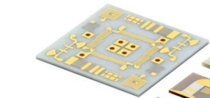
Ceramic PCBs
2. Ceramic PCB Manufacturing: Process Overview
Manufacturing Ceramic PCBs is a precise and complex process that demands accuracy at every stage. The major methods include:
2.1 Direct Bonded Copper (DBC)
This method bonds copper sheets directly onto a ceramic surface at high temperatures, usually above 1000°C. It is widely used in power electronics due to its excellent thermal and electrical performance.
2.2 Active Metal Brazed (AMB) Technology
AMB involves using an active metal (e.g., Ti, Zr) in brazing alloys to facilitate bonding between the ceramic and metal layers. Though costlier than DBC, AMB provides stronger adhesion and better reliability.
2.3 Low-Temperature Co-fired Ceramic (LTCC)
LTCC integrates multiple layers of ceramics and conductors, co-fired at temperatures around 850°C. It enables 3D circuit structures and is suitable for compact, high-frequency devices like RF modules.
3. Challenges in Manufacturing Ceramic PCB and Solutions
Manufacturing Ceramic PCB at scale brings forth a unique set of challenges. Below are some of the most critical issues faced by PCB factories and how they can be resolved.
3.1 Cracking and Warping During Sintering
Problem: Ceramic substrates are brittle and tend to crack or warp under thermal stress.
Solution: Controlled atmosphere sintering and gradual thermal ramp-up can reduce internal stresses. Utilizing matched CTE (Coefficient of Thermal Expansion) copper layers also helps.
3.2 Inconsistent Copper Adhesion
Problem: Achieving uniform copper bonding on a ceramic surface is more complex than on FR4.
Solution: Technologies like DBC and AMB, when optimized, ensure consistent metal adhesion. Surface treatment and oxide layer control also improve yield rates.
3.3 Difficulty in Multi-Layer Integration
Problem: Stacking multiple ceramic layers without compromising signal integrity or creating micro-cracks is challenging.
Solution: LTCC offers a robust multi-layer integration solution. Material and process control are essential for achieving reliability.
4. Types of Ceramic PCB: Choosing the Right Format
Understanding the different structural formats of Ceramic PCBs is key to optimizing their application:
4.1 DBC-Based Ceramic PCB
Used for high-power applications like LED drivers, automotive control systems, and power modules due to excellent heat dissipation.
4.2 HTCC and LTCC Ceramic PCB
HTCC (High-Temperature Co-fired Ceramic) is sintered at >1600°C and used in harsh environments, while LTCC is more flexible and supports embedded passive components.
4.3 Multilayer Ceramic PCB
Multilayer formats enable compact and complex designs in RF/microwave circuits and medical implants.
5. Applications of Ceramic PCB Across Industries
Ceramic PCBs are deployed in sectors where thermal performance, reliability, and miniaturization are essential.
5.1 Power Electronics
Inverters, converters, and IGBTs use Ceramic PCBs to handle high voltages and thermal loads.
5.2 LED Lighting Systems
The excellent heat dissipation of Ceramic PCBs makes them perfect for high-brightness LED assemblies.
5.3 Aerospace and Defense
Their stability under extreme temperature fluctuations makes them suitable for satellites, radar systems, and avionics.
5.4 Automotive Electronics
Advanced driver assistance systems (ADAS), electric vehicle power controls, and engine modules rely on Ceramic PCBs for robust performance.
SQ PCB provides customized Ceramic PCB solutions with rapid prototyping, making them a preferred partner for clients in aerospace and high-end automotive sectors.
7. Ceramic PCB Design Guidelines and Best Practices
The design of Ceramic PCB involves unique considerations due to the physical and electrical characteristics of ceramic substrates. Designers must balance electrical performance, mechanical durability, and thermal management.
7.1 Substrate Material Selection
When selecting the right ceramic substrate, the following factors should be evaluated:
-
Thermal Conductivity: AlN and BeO offer superior performance compared to Al₂O₃.
-
Dielectric Strength: Important for high-voltage applications.
-
Mechanical Strength: Ceramics can be brittle, requiring optimized layout to avoid mechanical stress concentration.
-
Coefficient of Thermal Expansion (CTE): Should closely match the copper conductor to prevent delamination.
7.2 Copper Thickness Optimization
Ceramic PCB designs often require thicker copper layers to handle higher current and dissipate heat effectively. Common copper thicknesses range from 35µm (1 oz) to 210µm (6 oz) depending on the power density.
However, thicker copper layers also increase cost and reduce etching resolution, so a trade-off must be considered.
7.3 Trace Width and Spacing
Due to better insulation and thermal conductivity, traces can be denser on Ceramic PCBs. However, the minimum trace width is still limited by the manufacturing process and etching capability.
Designers often apply the IPC-2221 standard to determine minimum trace width, spacing, and via dimensions.
7.4 Thermal Via Placement
For designs with concentrated heat generation, thermal vias can be embedded in the ceramic substrate to enhance heat conduction toward the heat sink or chassis.
7.5 Surface Finish Options
Common finishes compatible with Ceramic PCB include:
-
ENIG (Electroless Nickel Immersion Gold): Good for wire bonding and solderability.
-
Silver or Gold Thick Film: Often used in sensor applications.
-
OSP (Organic Solderability Preservative): Less common, but cost-effective for certain applications.
8. Ceramic PCB Testing and Quality Assurance Techniques
Due to their high-reliability applications, Ceramic PCBs undergo rigorous testing processes to ensure consistent performance and durability.
8.1 Thermal Cycling Test
This test simulates repeated exposure to thermal extremes. Ceramic PCB assemblies are cycled between -55°C and +125°C to evaluate:
-
Copper-ceramic adhesion
-
Delamination risks
-
Electrical performance over thermal shock
8.2 Dielectric Withstand Test
Also called high-pot testing, this test evaluates the insulation strength of the ceramic material by applying high voltage between conductors and substrate. Al₂O₃ typically withstands 10–15 kV/mm.
8.3 Surface Quality Inspection
Visual inspection, automated optical inspection (AOI), and X-ray are used to detect:
-
Surface cracks or voids
-
Metallization defects
-
Internal misalignment of layers (especially in LTCC/HTCC)
8.4 Mechanical Strength Testing
Mechanical shock and vibration tests are conducted for Ceramic PCB used in aerospace, automotive, or defense environments.
8.5 Electrical Parameter Testing
Each PCB is tested for impedance, capacitance, resistance, and signal integrity under realistic operation conditions to ensure conformity to design values.
9. Cost Structure and Supply Chain Analysis of Ceramic PCB
The cost of producing a Ceramic PCB is higher than FR4, due to both materials and processing requirements. Understanding this cost breakdown helps in optimizing supply chain decisions.
9.1 Material Cost
Ceramic substrates (especially AlN and BeO) are significantly more expensive than FR4, primarily due to:
-
Purity requirements
-
Manufacturing scale limitations
-
Export regulations (particularly for BeO)
Copper costs are higher too due to the need for thick or directly bonded copper.
9.2 Processing and Yield Costs
Manufacturing Ceramic PCBs involves high-temperature sintering, cleanroom requirements, and low yield due to the brittle nature of ceramics. The added difficulty in handling results in:
-
Increased waste
-
Higher inspection and QA costs
-
Expensive tooling and automation systems
9.3 Equipment and Capital Expenditure
Specialized machinery such as:
-
Laser cutters for brittle ceramic panels
-
Sputtering equipment for thin film metallization
-
High-precision screen printers for thick film circuits
These capital investments are reflected in the final price.
9.4 Lead Time and Supply Chain Considerations
Lead times are longer for Ceramic PCB due to:
-
Limited global suppliers of high-grade ceramic substrates
-
Customization needs for most applications
-
Intensive inspection cycles
Conclusion: Ceramic PCB as the Backbone of Next-Gen Electronics
Ceramic PCBs are no longer niche components used solely in defense or aerospace—they are becoming foundational to industries that demand performance, durability, and thermal efficiency. From the AI revolution to the rise of electric transportation, the reliability and robustness of Ceramic PCBs unlock design possibilities that traditional PCBs simply cannot support.
For product engineers and sourcing managers, investing in Ceramic PCB is not just about solving thermal problems—it’s about preparing for a future of smaller, faster, and more complex electronics.
1. What is the difference between rolled copper foil and electrolytic copper foil?
Rolled copper foil is produced by mechanically compressing copper, providing better surface finish and mechanical durability. Electrolytic copper foil is made through electro-deposition, offering flexibility and being more cost-effective.
2. Can Ceramic PCBs replace all FR4 PCBs?
No, Ceramic PCBs are more expensive and are used where FR4 cannot meet thermal or frequency demands. They’re complementary, not replacements.
3. How do you ensure thermal conductivity in Ceramic PCB design?
Selecting high-conductivity materials like AlN and optimizing copper layer thickness are key to enhancing thermal performance.
4. Are Ceramic PCBs environmentally friendly?
Yes, particularly Al₂O₃ and AlN are non-toxic and recyclable, but BeO requires caution due to its toxic nature.
5. What is the typical thickness of a Ceramic PCB substrate?
Substrate thickness usually ranges from 0.25mm to 1.0mm, depending on application requirements and thermal management needs.

- long board pcb
- Flexible PCBs
- Special PCB
- Express Printed Circuit Board
- Pcb Prototype
- LED PCB
- PCB
- Printed Circuit Board
- Pcb meaning
- Pcb manufacturer
- Rigid pcb board
- Rigid Flex PCB
 Quote
Quote
 E-mail